What is a GaN Charger? Gallium Nitride vs. Silicon Technology Complete Guide
Have you ever wondered why your laptop’s power brick feels like a literal “brick” in your backpack, or why your phone charger gets hot enough to cook an egg while fast-charging? For decades, we accepted these inconveniences as the price of power. But a silent revolution in material science has changed the game.
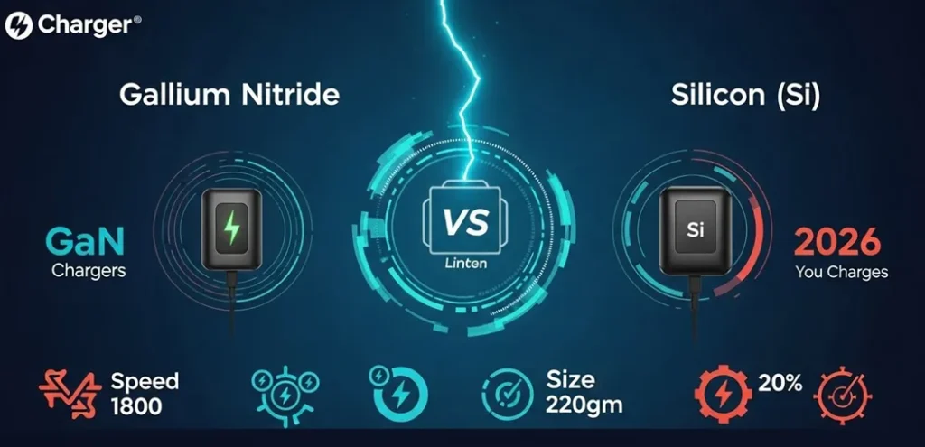
The era of Silicon (Si) dominance is ending, and the era of Gallium Nitride (GaN) has arrived. This isn’t just a minor upgrade; it’s a fundamental shift in how electricity is managed. In this comprehensive guide, we will dissect the physics, the economics, and the practical utility of GaN technology to explain why your next charger must be a GaN charger.
1. The Hook: Why Your Old Silicon Charger is Failing You
To understand the solution, you must understand the problem. Traditional chargers use silicon-based transistors. While silicon is the most abundant semiconductor on Earth, it has a “thermal bottleneck.”
When you try to push high wattage (like 65W or 100W) through silicon, it resists. That resistance generates heat. To prevent the charger from melting, manufacturers have to add bulky heat sinks and leave “dead space” inside the casing for airflow. This is why high-power silicon chargers are massive and heavy. GaN solves this by virtually eliminating that resistance.
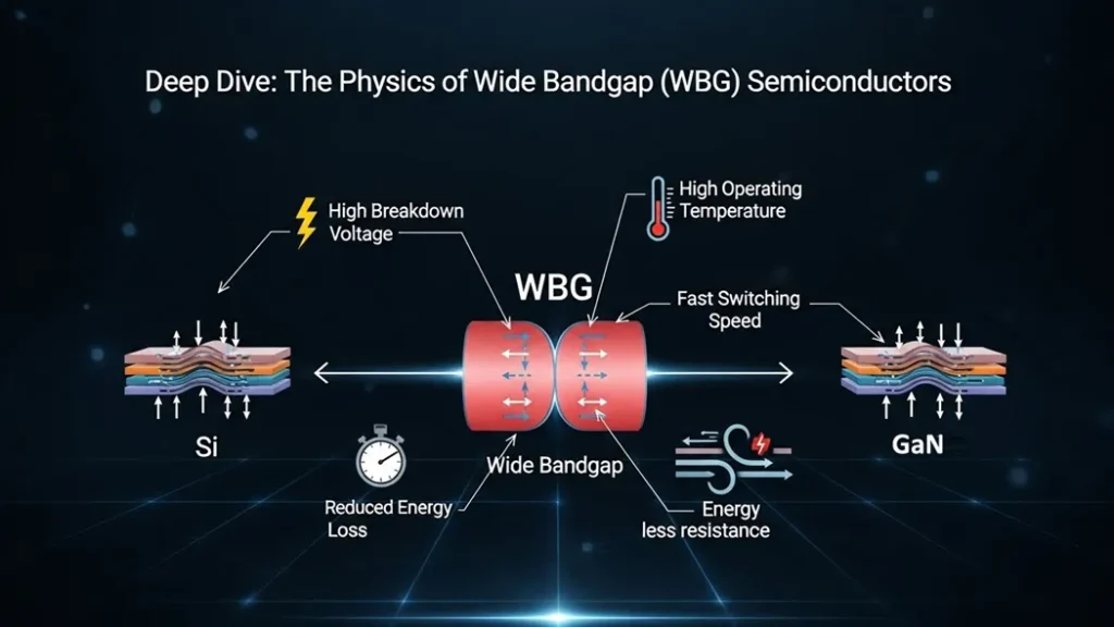
2. Deep Dive: The Physics of Wide Bandgap (WBG) Semiconductors
To achieve an “Encyclopedia” level of depth, we must look at the atomic level. The performance of a semiconductor is defined by its Bandgap.
The Electron Leap
In any semiconductor, there is a “Valence Band” (where electrons stay) and a “Conduction Band” (where electrons move to create current). The space between them is the Bandgap.
Silicon’s Bandgap:
Eg(Si)=1.12 eV
GaN’s Bandgap:
Eg(GaN)=3.4 eV
Because GaN’s bandgap is three times wider than silicon’s, it can handle much higher electrical fields. Imagine a bridge: Silicon is a wooden footbridge that collapses under a heavy truck (high voltage). GaN is a reinforced steel bridge that handles the same truck without breaking a sweat.
Electron Mobility
GaN electrons move 30% faster than silicon electrons. In the world of high-speed switching, this means the charger can “pulse” electricity at incredible frequencies. High-frequency switching allows us to use much smaller transformers and inductors—the two bulkiest parts of any charger.
3. The “Problem-Solver” Angle: Solving the Modern Tech Dilemma
Modern users face a “Port Paradox”: we have more devices than ever (phone, watch, buds, laptop, tablet), but we want less clutter.
The Death of the Proprietary Brick
In the past, every laptop had a specific, heavy power brick. If you lost it, you were in trouble. GaN technology, combined with USB-C Power Delivery (PD), has created a universal charging standard. A high-quality 100W GaN charger can intelligently identify whether it’s plugged into a low-power pair of AirPods (drawing 2.5W) or a high-power MacBook Pro (drawing 96W).
Eliminating “Vampire Power”
Standard silicon chargers often suffer from “No-Load Power Consumption”—they pull electricity from the wall even when your phone is disconnected. GaN’s superior efficiency significantly reduces this “vampire” drain, making your home more energy-efficient and lowering your electricity bill over time.
4. Performance Metrics: A Head-to-Head Comparison
| Technical Metric | Silicon (Legacy) | Gallium Nitride (GaN) |
|---|---|---|
| Power Density | Low (~5-8 Watts per in³) | High (~15-25 Watts per in³) |
| Breakdown Voltage | ~600V (Limited) | ~1000V+ (Robust) |
| Thermal Conductivity | Average | Superior |
| Switching Losses | Significant (Turns into heat) | Minimal (Stays as power) |
| System Cost | Low (Material cost) | Moderate (Higher upfront, lower TCO) |
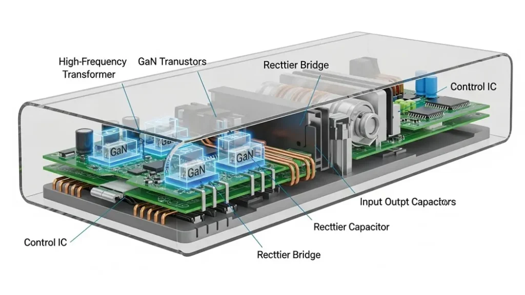
5. The Architecture of a GaN Charger: What’s Inside?
An encyclopedia-style look at the internal components reveals why GaN is so revolutionary:
- The GaN FET (Field-Effect Transistor): This is the heart of the device. It replaces the silicon MOSFET. It’s smaller, faster, and cooler.
- Planar Transformers: Instead of bulky wire-wrapped iron cores, many GaN chargers use “planar” transformers—flat circuits that are incredibly thin but highly efficient.
- Controller IC: A sophisticated logic chip that manages “Handshaking.” It “talks” to your device to negotiate voltage (5V, 9V, 15V, or 20V) to prevent overcharging.
- EMI Shielding: Because GaN operates at higher frequencies, it can produce electromagnetic interference. High-end GaN chargers use advanced shielding to ensure they don’t interfere with your Wi-Fi or radio signals.

6. Industry Use-Cases: Beyond the Smartphone
While we mostly see GaN in wall chargers, its impact is broader:
- Data Centers: GaN reduces cooling costs in massive server farms.
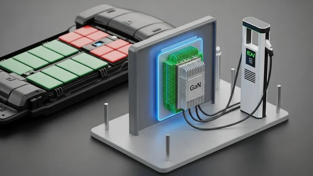
- Electric Vehicles (EVs): GaN inverters make EV chargers faster and the cars themselves lighter.
- 5G Infrastructure: GaN is used in 5G base stations to handle the high-frequency radio waves more efficiently than silicon.
7. The Economics: Why is it more expensive?
You will notice GaN chargers cost 2x more than standard ones. This is because growing GaN crystals is a complex process. Unlike silicon, which can be grown in massive “boules,” GaN is usually grown on a substrate (like sapphire or silicon) using a process called Epitaxy.
However, when you factor in the Total Cost of Ownership (TCO)—one charger replacing three, less heat damage to your expensive phone battery, and lower energy waste—GaN is actually the cheaper option in the long run.
8. Frequently Asked Questions (The Ultimate FAQ)
Q1: Can a GaN charger “fry” my old, non-fast-charging phone?
No. This is a common myth. The GaN charger doesn’t “push” power; the device “pulls” it. If you plug a 10-year-old phone that only supports 5W into a 140W GaN charger, the charger’s PD (Power Delivery) chip will recognize the device and only provide exactly 5W. It is 100% safe.
Q2: Why does my GaN charger “re-handshake” (disconnect/reconnect) when I plug in a second device?
This is a feature, not a bug. When you add a second device, the GaN controller must recalculate the power distribution. It briefly cuts power to “re-negotiate” the wattage with both devices to ensure neither gets too much or too little voltage. This is called Dynamic Power Allocation.
Q3: Does GaN technology improve battery health?
Indirectly, yes. Heat is the primary cause of lithium-ion battery degradation. Because GaN chargers deliver a much “cleaner” and more stable current with less heat transfer through the cable, your phone’s internal charging circuitry stays cooler. A cooler battery lasts for more charge cycles.
Q4: Are “GaN II” and “GaN III” real, or just marketing?
They are real. “GaN II” generally refers to the integration of the driver and the GaN FET into a single chip (using technology like Power Integrations’ InnoSwitch). This further reduces size and increases switching frequency. GaN III/GaNPrime usually introduces even better safety protocols and even higher efficiency (up to 97%).
Q5: Can I use a 100W GaN charger with a cheap $2 cable?
Highly discouraged. While the charger is smart, a cheap cable lacks an E-Marker chip. To pull more than 60W (3A), you must use a cable rated for 5A (100W) with an E-Marker chip. Using a basic cable will limit your charging speed to 60W, regardless of how powerful the charger is.
Q6: Do GaN chargers make noise?
High-quality GaN chargers are silent. However, because they operate at high frequencies, some low-quality units may exhibit “coil whine”—a high-pitched buzzing. If your GaN charger makes a loud noise, it may have poor EMI shielding or a failing capacitor.
9. Final Verdict: The Professional Recommendation
If you are an enthusiast, a professional, or simply someone who values their time, the transition to GaN is inevitable.
Our Recommendation: Purchase a 65W or 100W GaN 3-Port Charger. It is the “Goldilocks” of power—enough to charge a laptop at full speed, yet small enough to fit in a jacket pocket.
The silicon era was great for getting us here, but Gallium Nitride is the material that will power our future.