Full Wave Rectifier: Working Principle, Circuit Types, Formulas & Efficiency Guide
The definitive engineering guide from AC-to-DC conversion fundamentals to bridge vs center-tapped circuits, efficiency derivations, PIV calculations, filter design, diode selection, and IEC 60146 compliance.
🎯 Key Takeaways
- ✅ A full wave rectifier converts both halves of the AC waveform into pulsating DC doubling output frequency and halving ripple compared to a half-wave design
- ✅ Theoretical maximum efficiency is 81.2% exactly double the 40.6% of a half-wave rectifier governed by the formula η = 0.812 / (1 + Rf/RL)
- ✅ Ripple factor is 0.48 for full-wave vs 1.21 for half-wave a 2.5× smoother DC output that dramatically reduces filter capacitor size requirements
- ✅ Bridge rectifier (4 diodes, PIV = Vm) vs center-tapped (2 diodes, PIV = 2Vm) bridge preferred for high-voltage applications; center-tapped for lower forward-drop losses
- ✅ Filter capacitor sizing: C = Iload / (2 × f × ΔV) full-wave’s doubled ripple frequency (2f) means the required capacitance is half that needed for an equivalent half-wave circuit
- ✅ Diode selection requires evaluating both PIV rating (breakdown protection) and IFSM surge current (capacitor inrush protection) both must be derated by at least 20% in design
- ✅ Standards compliance: IEC 60146 (semiconductor converters), IEC 62368-1 (power supply safety), and IEEE 519 (harmonic distortion limits) govern professional rectifier design
Figure 1: Full wave rectifier overview both circuit topologies convert the complete AC cycle into pulsating DC output.
What Every Electronics Engineer Must Know About Full-Wave Rectification
Full-wave rectification produces ripple at 2× the input frequency (120 Hz from 60 Hz mains). This is why filter capacitors and inductors are smaller they have to handle shorter ripple periods between charge cycles.
Bridge rectifiers use 4 diodes (2× forward drops in series) but need no center-tap transformer. Center-tapped use only 2 diodes (1× forward drop) but require a more expensive transformer. Choose based on transformer cost vs. diode loss budget.
At power-on, a discharged filter capacitor looks like a short circuit. The resulting inrush current spike can be 10–100× the rated DC current. Always verify the diode’s IFSM (peak surge current) rating exceeds this worst-case value.
What is a full wave rectifier?
A full wave rectifier is basically a circuit that converts an AC signal into DC, but instead of wasting half the signal like a half-wave rectifier, it uses both the positive and negative cycles. Because of that, the output is more continuous (though still a bit pulsating, not perfectly smooth). Its efficiency is around 81% (theoretical), and one interesting thing is the output frequency becomes double the input frequency. The ripple factor is about 0.48, so yeah, there’s still some fluctuation in the output, but it’s generally acceptable for most uses.You’ll find full wave rectifiers almost everywhere in power supplies, battery chargers, audio systems, etc. Basically any place where AC needs to be turned into DC. There are two main types:* Center-tapped rectifier (uses 2 diodes and a transformer with a center tap) * Bridge rectifier (uses 4 diodes and doesn’t need a center tap)So overall, it’s a pretty standard and widely used way to convert AC into usable DC.📋 Table of Contents
- Introduction to Full Wave Rectifiers
- Working Principle of Full Wave Rectification
- Key Circuit Types: Center-Tapped vs Bridge Rectifier
- Output Waveform Analysis & Filtering
- Technical Calculations: All 10 Formulas Explained
- Quantitative Diode Selection: PIV, IFSM & Thermal Rating
- Full Wave vs Half Wave Rectifier: Complete Comparison
- Advantages & Disadvantages
- Real-World Applications in Electronics
- Design Standards & Industry Compliance (IEC/IEEE)
- Troubleshooting: Fault Diagnosis Guide
- Step-by-Step Build Guide & Experiment
- 13 Expert FAQs
Introduction to Full Wave Rectifiers
In real-world electronics converting AC to DC is one of those things I keep running into all the time. Almost every setup I’ve worked on whether it’s a small charger or a proper power supply has some kind of rectifier in it. Personally, I tend to go with a full wave rectifier most of the time. It just makes more sense since it uses both halves of the AC signal instead of wasting one. I remember when I first compared it with a half-wave setup, I didn’t fully get the difference… but once I actually looked at the output on an oscilloscope, it kind of clicked. The waveform is just more usable.In practical installations, I’ve rarely seen engineers choose half-wave unless there’s a specific limitation. From what I’ve seen, full wave designs are just more reliable overall. Yeah, they can be slightly more complex, but the output quality is usually worth it. In this guide, I’m trying to explain things in a way that actually makes sense without overloading everything with theory. I’ve noticed that when explanations get too perfect or too structured, they become harder to follow. So this is a bit more relaxed and experience-based.
There’s also some history behind all this. I don’t always focus on that part myself, but it’s interesting to know that these rectifier concepts go way back to the late 1800s. What we use today is just a much more refined version of those early ideas. Before going further, I’d say it helps if you already have a basic fundamentals of electronic circuits. Nothing too deep just enough so things don’t feel confusing as you read along.
Working Principle of Full Wave Rectification
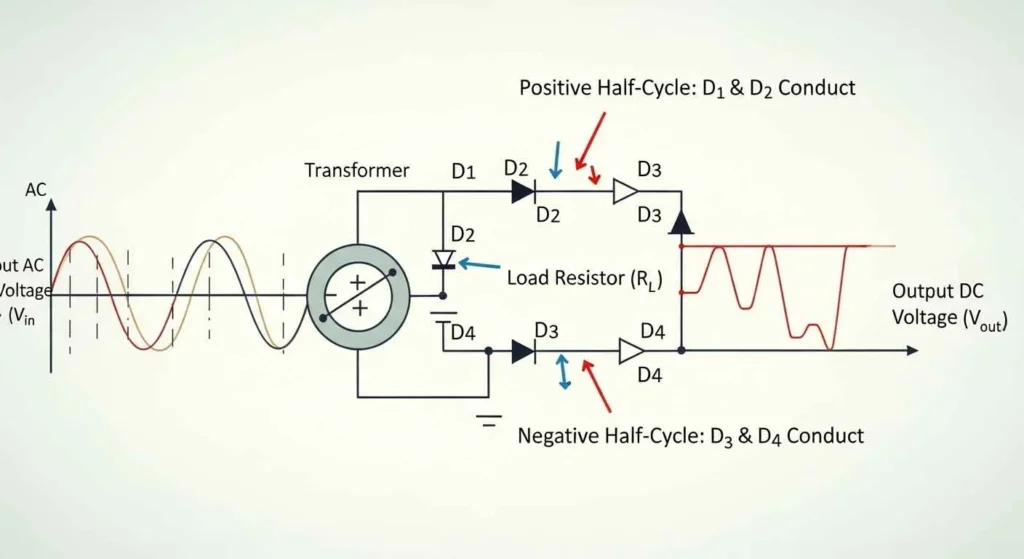
Figure 2: Current path through the bridge rectifier during positive half-cycle (D1, D3 conduct) and negative half-cycle (D2, D4 conduct) load current flows in the same direction in both cases.
The operation of a full wave rectifier is rooted in the unidirectional conduction property of the p-n junction diode. A diode conducts current only when its anode is at a higher potential than its cathode (forward biased) and blocks current completely when reverse biased. The full wave rectifier exploits this property with either two or four diodes arranged so that current through the load resistor always flows in the same direction regardless of whether the AC input is in its positive or negative half cycle.
Bridge Rectifier Operation (4-Diode)
In the bridge configuration, four diodes (D1–D4) are arranged in a closed loop. The AC source connects across two opposite nodes of the bridge; the load connects across the other two. During the positive half cycle, diodes D1 and D3 are forward biased and conduct. Current flows from the positive AC terminal, through D1, through the load (top to bottom), through D3, and back to the negative AC terminal. During the negative half cycle, the polarity reverses: D2 and D4 conduct while D1 and D3 block. Current again flows through the load in the same direction top to bottom even though the source polarity has reversed. The result is a pulsating DC output at twice the input frequency.
Center-Tapped Rectifier Operation (2-Diode)
The center-tapped design uses a transformer with a center-tap on the secondary winding, which serves as the circuit reference (ground). Each diode connects to one end of the secondary winding. During the positive half cycle, the upper half of the winding is positive: D1 conducts and current flows through the load. During the negative half cycle, the lower half becomes positive: D2 conducts and current again flows through the load in the same direction. The center tap ensures the voltage seen by each diode is only half the total secondary voltage but this comes at the cost of doubling the PIV requirement.
Compare to half-wave: Vdc = Vm/π ≈ 0.318 × Vm full wave produces exactly double the average voltage
Example: 12Vrms secondary → Vm = 12 × √2 = 16.97V → Vdc = 2 × 16.97 / π = 10.8V DC (before filter capacitor)
Key Circuit Types: Center-Tapped vs Bridge Rectifier
Center-Tapped Full Wave Rectifier

Figure 3: Center-tapped full wave rectifier two diodes alternate conduction on each half cycle, with the transformer center-tap as the DC ground reference.
From what I’ve seen, the center-tapped full wave rectifier has one clear advantage it only uses two diodes. That might not sound like a big deal at first, but in practice, it actually reduces the voltage drop compared to a bridge rectifier. Instead of losing voltage across two diodes, you’re only dealing with one. I remember when I was first working with low-voltage supplies, this started to matter a lot more than I expected. Like, if you’re dealing with something around 5V, even a 0.7V drop is kind of a big hit. That’s roughly 14% gone, which honestly feels like a lot. But at higher voltages, say 100V, the same drop barely makes a difference so it’s not always a concern.
In real-world designs, especially low-voltage ones, I’ve noticed engineers try to reduce this loss as much as possible. That’s where things like Schottky diodes come in, since they have a lower forward voltage. And in more advanced setups, I’ve seen synchronous rectification used as well using MOSFETs instead of diodes. It’s a bit more complex, but yeah, the voltage drop gets really small. That said, the center-tapped design isn’t perfect. One thing I’ve personally had to be careful about is the voltage stress on the diodes. The non-conducting diode has to handle a much higher reverse voltage about twice the peak value of the input. So you can’t just pick any diode, you actually need a higher voltage rating compared to what you’d use in a bridge rectifier. So yeah, it’s kind of a trade-off. You gain efficiency in one place, but you have to be more careful somewhere else. That’s usually how it goes with these circuits..
Full Wave Bridge Rectifier
Figure 4: Bridge rectifier four diodes in a diamond arrangement. No center-tap transformer required; PIV per diode equals only Vm.
The bridge rectifier is the dominant topology in modern power supply design for three reasons: it requires no center-tap transformer (significantly reducing transformer cost and size at higher voltages), each diode only needs to withstand a PIV of Vm (half that of the center-tapped design), and the transformer utilization factor (TUF) of 0.812 means the transformer is used more efficiently, allowing smaller core sizes. The sole disadvantage two forward voltage drops in series (2 × Vf ≈ 1.4V for silicon diodes) is irrelevant in most practical designs where output voltages exceed 20V. Below 5V, however, synchronous rectification or Schottky diodes are standard practice.
| Parameter | Center-Tapped | Bridge Rectifier | Winner |
|---|---|---|---|
| Number of Diodes | 2 | 4 | Center-Tapped |
| Forward Drop Loss | 1 × Vf ≈ 0.7V | 2 × Vf ≈ 1.4V | Center-Tapped |
| PIV per Diode | 2 × Vm | Vm | Bridge |
| Transformer | Center-tap required (costly) | Simple secondary winding | Bridge |
| TUF | 0.672 (poor utilization) | 0.812 (better utilization) | Bridge |
| Best Use Case | Low-voltage (<5V) supplies, audio | High-voltage, general purpose | |
| Efficiency (η) | ~81.2% | ~81.2% | Equal |
| Ripple Factor | 0.48 | 0.48 | Equal |
Output Waveform Analysis & Filtering
Figure 5: Unfiltered full wave output (top) positive humps at 2× frequency. With capacitor filter (bottom) ripple voltage ΔV depends on load current and capacitor value.
The unfiltered output of a full wave rectifier is a series of positive half-sine “humps” at twice the input frequency. Without a filter, this pulsating DC would cause audible hum in audio equipment, heat in DC motors, and instability in logic circuits. The three standard filtering approaches capacitor (C-filter), capacitor-inductor (LC-filter), and voltage regulator IC each serve different application requirements.
Capacitor (C-Filter): The Standard Approach
A large electrolytic capacitor connected across the load provides the most common filtering method. Between each rectified pulse, the capacitor charges to the peak voltage, then slowly discharges into the load until the next pulse recharges it. The voltage drop between peaks is the ripple voltage (ΔV).
f = AC input frequency (Hz) | 2f = ripple frequency for full-wave (e.g. 120 Hz at 60 Hz mains)
ΔV = Acceptable peak-to-peak ripple voltage (Volts)
Example: 1A load, 60 Hz mains, 0.5V ripple → C = 1.0 / (2 × 60 × 0.5) = 16,667 μF ≈ 22,000 μF (standard value)
Half-wave equivalent: C = 1.0 / (1 × 60 × 0.5) = 33,333 μF full wave needs half the capacitance!
LC Filter: For High-Current Industrial Loads
For power supplies driving heavy resistive or inductive loads where ripple must be minimised motor controllers, audio amplifiers, electroplating rectifiers an LC (inductor-capacitor) filter provides substantially better ripple rejection than a capacitor alone. The series inductor opposes rapid changes in current (by Lenz’s Law), smoothing the current drawn from the rectifier stage. This prevents the large current spikes that degrade efficiency and capacitor life in pure C-filter designs. The LC filter is standard in industrial power supplies rated above 5A continuous output.
Voltage Regulator ICs: For Precision DC Outputs
After C or LC filtering, a linear regulator IC provides the final precision regulation. The LM78xx series (LM7805 for 5V, LM7812 for 12V, LM7815 for 15V) are the industry-standard workhorses. They convert the filtered, slightly unsteady DC into a precise, temperature-stable output voltage. The critical design constraint is dropout voltage: the rectified and filtered input must always exceed the desired output by at least 2–3V for the regulator to maintain control. For a 12V regulated output, the filter capacitor voltage must never drop below approximately 14.5–15V under maximum load.
Design Tip: Always Add Voltage Margin
When sizing your transformer secondary voltage, account for: diode forward drops (1.4V for silicon bridge), voltage drop across the series inductor if used, regulator dropout voltage (typically 2–3V for LM78xx), and worst-case capacitor ripple at maximum load. A 12V regulated output from a bridge rectifier with LM7812 typically requires a transformer secondary of at least 15–16Vrms. Tighter designs use low-dropout (LDO) regulators (dropout 0.3–0.5V) or switch to SMPS topologies for higher efficiency.
Technical Calculations: All 10 Formulas Explained
Figure 6: The mathematical framework of full wave rectifier analysis ten interrelated formulas from average DC voltage to transformer utilization factor.
Vm = Peak voltage of AC secondary (= Vrms × √2) | Practical: subtract diode forward drops (2×0.7V for bridge)
Practical Vdc (bridge) = (2Vm/π) − 1.4V
Used to calculate actual power dissipated in resistive loads: P = Vrms² / RL
Maximum theoretical: ηmax = 81.21% (when Rf → 0, ideal diodes and transformer)
Exactly double the half-wave maximum of 40.6% because full wave uses both half cycles
Full wave: γ = 0.48 | Half wave: γ = 1.21 | Perfect DC: γ = 0
Lower γ = smoother output. A γ of 0.48 means the AC ripple amplitude is 48% of the DC level (unfiltered)
Bridge: each diode shares the reverse voltage, so PIV = Vm
Center-tapped: the non-conducting diode sees the full secondary voltage, so PIV = 2Vm
Design rule: Select diodes with VRRM ≥ 1.2 × PIV (20% safety derating minimum)
Closer to 1.0 = more ideal DC output. Used in transformer rating calculations.
Bridge’s TUF of 0.812 is significantly better than center-tapped’s 0.672 a 21% transformer size advantage
This is a primary reason bridge rectifiers dominate in cost-sensitive designs
Half wave: ripple frequency equals supply frequency (60 Hz or 50 Hz)
Doubled frequency: filter components (C and L) work twice as often per second requiring half the value for equivalent ripple reduction
Idc = Vdc / RL = (2Vm/π) / RL
Used to verify the power handling requirement of the load resistor and verify efficiency calculation
The factor 2f (doubled frequency) is unique to full-wave it’s what makes the capacitor requirement half that of a half-wave circuit
Always select electrolytic capacitors with a voltage rating ≥ 1.25 × Vm for safety margin
Given: 12Vdc regulated output, 1A load, 60 Hz mains, 0.5V maximum ripple, LM7812 regulator (2.5V dropout).
Step 1 Minimum filter capacitor voltage: 12V + 2.5V (dropout) + 0.5V (ripple margin) = 15V minimum.
Step 2 Required peak voltage: 15V + 1.4V (bridge drops) = 16.4V peak → transformer secondary = 16.4/√2 = 11.6Vrms use standard 12Vrms secondary.
Step 3 Actual peak: 12 × √2 − 1.4V = 15.6V peak (satisfactory, ≥15V needed).
Step 4 Capacitor: C = 1.0 / (2 × 60 × 0.5) = 16,667 μF → use 22,000 μF / 25V.
Step 5 Diode PIV rating: PIV = Vm = 16.97V × 1.2 safety factor = 20.4V → use 1N4007 (1000V PIV, 1A) very conservative and standard practice.
Quantitative Diode Selection: PIV, IFSM & Thermal Rating
Figure 7: Full wave rectifier in a complete DC power supply transformer, bridge rectifier, filter capacitor, and voltage regulator IC stages.
Selecting the correct diode is one of the most critical and most overlooked aspects of rectifier design. Three parameters must all be satisfied simultaneously: reverse voltage rating (VRRM), average forward current (IF(avg)), and peak surge current (IFSM).
Reverse Voltage Rating (VRRM)
As established in the PIV formula, the diode must withstand the peak reverse voltage without breakdown. Always apply a safety derating factor of at least 20% (some engineers use 50% for industrial reliability). For a 12Vrms secondary bridge rectifier (Vm = 16.97V), the minimum VRRM = 16.97 × 1.2 = 20.4V. The 1N4007 (1000V) is the standard low-cost choice even though 40V would theoretically suffice the over-spec costs nothing and provides margin against transient voltage spikes from inductive loads.
Surge Current Rating (IFSM)
This is the most commonly underappreciated parameter. When a power supply is first switched on with a discharged filter capacitor, the capacitor initially acts as a short circuit. The resulting inrush current is limited only by the transformer winding resistance and the diode forward resistance and can be 10 to 100× the rated DC output current. The 1N4007 has an IFSM of 30A which is why it is routinely used in 1A power supplies despite being rated for 1A average current. For higher-power designs, NTC thermistors (inrush current limiters) in series with the AC input are used to protect diodes and transformers.
| Diode Type | VRRM | IF(avg) | Vf @ IF | IFSM | Best Application |
|---|---|---|---|---|---|
| 1N4001 | 50V | 1A | 1.1V @ 1A | 30A | Low-voltage (up to 35Vrms) general purpose |
| 1N4007 Most Common | 1000V | 1A | 1.1V @ 1A | 30A | Universal standard mains rectification, any voltage |
| 1N5408 | 1000V | 3A | 1.2V @ 3A | 200A | Medium-power supplies (up to 3A continuous) |
| MBR1045 Schottky | 45V | 10A | 0.55V @ 5A | 150A | Low-voltage SMPS, PC power supplies low forward drop |
| SiC Diode (e.g. C3D10060) | 600V | 10A | 1.5V @ 10A | Low (SiC characteristic) | High-frequency EV chargers, PFC stages near-zero reverse recovery |
| GBPC3510 Bridge Module | 1000V | 35A | 1.1V @ 35A | 700A | Industrial power supplies, motor drives integrated 4-diode module |
I once debugged a 5V/10A bench power supply where diodes were failing intermittently despite being correctly rated for average current. The culprit was the inrush current at power-on the 22,000 μF filter capacitor was charging through the bridge in under 2 milliseconds, creating a current spike that exceeded the diode IFSM rating on every power cycle. Adding a 3Ω NTC inrush limiter in series with the AC input reduced the peak inrush from 80A to under 25A and the diode failures stopped immediately. Always calculate inrush, not just rated current.
Full Wave vs Half Wave Rectifier: Complete Comparison
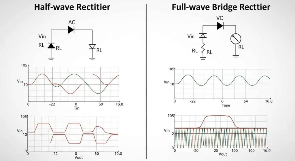
Figure 8: Half wave vs full wave rectifier comparison efficiency, ripple factor, output frequency, and component requirements at a glance.
| Feature | Half-Wave | Full-Wave (CT) | Bridge Rectifier |
|---|---|---|---|
| AC Utilization | One half cycle only | Both half cycles | Both half cycles |
| Efficiency (η) | ~40.6% Poor | ~81.2% Good | ~81.2% Good |
| Ripple Factor (γ) | 1.21 High ripple | 0.48 Low ripple | 0.48 Low ripple |
| Output Frequency | f (e.g. 60 Hz) | 2f (e.g. 120 Hz) | 2f (e.g. 120 Hz) |
| Average Vdc | Vm/π ≈ 0.318 Vm | 2Vm/π ≈ 0.637 Vm | 2Vm/π − 1.4V |
| Transformer | Simple | Center-tap required | Simple secondary |
| PIV per Diode | Vm | 2Vm High | Vm Low |
| TUF | 0.287 Poor | 0.672 | 0.812 Best |
| Filter Cap Size | Large (f ripple freq) | Small (2f ripple freq) | Small (2f ripple freq) |
| Primary Applications | Simple low-power, signal demodulation | Low-voltage audio, vintage gear | Universal SMPS, battery chargers, motor drives |
Advantages & Disadvantages
✅ Advantages of Full Wave Rectifiers
- 81.2% efficiency double that of half-wave; less energy wasted as heat in the rectifier stage
- Low ripple factor (0.48) smoother DC output requiring smaller, cheaper filter components
- Double output frequency (2f) filter capacitors and inductors work twice as hard per second, halving required component values
- Better transformer utilization (TUF = 0.812) no DC saturation of transformer core; smaller transformer for same power
- Higher average output voltage (0.637Vm vs 0.318Vm) nearly twice the average DC voltage from the same transformer
- Excellent compatibility with switch mode power supply designs forms the front-end rectifier stage in virtually all SMPS topologies
- Zener diode integration for simple voltage regulation with minimal added complexity
⚠️ Disadvantages of Full Wave Rectifiers
- More diodes required 4 diodes (bridge) vs 1 diode (half-wave); increased component count and cost (marginal in practice)
- Two forward drops in bridge 1.4V lost to diode drops, significant in low-voltage (<5V) designs
- Center-tapped design needs expensive transformer center-tap transformers cost 20–40% more than equivalent single-secondary types
- Higher PIV for center-tapped 2Vm requirement demands more expensive, higher-rated diodes
- Surge current at power-on large filter capacitors create high inrush current that can stress diodes and transformers if not managed
- Heat generation at high power diode forward drops dissipate P = Iload × 1.4W per amp in a bridge circuit; heat sinking required above ~3A
Real-World Applications in Electronics
Figure 9: Full wave rectifier applications span every sector of electronics from consumer chargers to industrial motor drives and medical instrumentation.
DC Power Supplies (All Electronics)
The bridge rectifier is the universal front-end of every AC-DC power supply. In linear supplies (lab power supplies, audio amplifiers, legacy equipment), the rectifier directly follows the mains transformer and feeds the filter capacitor and regulator stage. In switch mode power supplies (laptop chargers, LED drivers, industrial equipment), the bridge rectifier converts mains AC to raw DC which is then processed by a PWM controller, usually a MOSFET switching stage, for high-efficiency regulation. Understanding power supply classification helps contextualize where the rectifier fits in the complete power chain.
Battery Chargers
Battery chargers require both efficiency and current surge handling. Full wave rectifiers typically using 1N5408 (3A) or GBPC-series bridge modules for higher current provide the raw DC that the charging controller regulates. Schottky diodes are standard in fast chargers and USB-C PD adapters where the 1.4V bridge drop in a standard silicon bridge would represent an unacceptable efficiency loss at 5V output.
Audio Amplifiers
High-fidelity audio amplifiers are particularly sensitive to power supply ripple even small AC ripple superimposed on the supply rails creates audible hum at 100 or 120 Hz. The center-tapped full wave rectifier with very large filter capacitors (often 10,000–100,000 μF per rail) is traditional in linear audio supplies due to its single forward drop advantage. Bridge rectifiers are used where the extra 0.7V drop is acceptable, typically in amplifiers with supply rails above ±20V.
Industrial Motor Drives
Three-phase bridge rectifiers (6-pulse) form the input stage of variable frequency drives (VFDs) for industrial motors like the squirrel cage induction motor. The six-pulse rectifier reduces ripple frequency to 6× the supply frequency, making filtering easier. Active front-end (AFE) rectifiers using IGBTs replace passive diode bridges in regenerative drives, enabling energy recovery during braking.
Medical Devices
Medical-grade power supplies require double or reinforced insulation between AC mains and patient-accessible DC outputs per IEC 60601-1. Bridge rectifiers with appropriately isolated transformers provide the required 4kV or 8kV isolation barriers. Schottky diodes minimize forward drop losses and reduce heat generation in portable medical equipment where thermal management is critical.
Renewable Energy Systems
Rectifiers convert the AC output of wind turbines and variable-frequency AC generators to DC for battery storage or grid inverter input. Silicon Carbide (SiC) diodes with near-zero reverse recovery charge are displacing silicon in high-power renewable applications due to their dramatically lower switching losses at the elevated frequencies (tens of kHz) used in modern power conversion systems.
Design Standards & Industry Compliance (IEC/IEEE)
| Standard | Scope | Key Requirement for Rectifier Design |
|---|---|---|
| IEC 60146 Core Standard | Semiconductor converters general requirements and line-commutated converters | Performance and test requirements for rectifiers including efficiency measurement, voltage regulation, and protection coordination |
| IEC 62368-1 Safety | Safety of audio/video, IT and communications equipment (replaces IEC 60950-1) | Insulation requirements, creepage/clearance distances, thermal protection, fusing requirements for all mains-connected power supplies |
| IEEE 519 | Harmonic control in electric power systems | Sets limits on Total Harmonic Distortion (THD) injected back into the power grid; drives PFC (Power Factor Correction) requirements in mains rectifiers above 75W |
| IEC 61000-3-2 | Electromagnetic compatibility limits for harmonic current emissions | Classifies equipment into Classes A–D; Class D (PCs, monitors, TVs) has the most stringent harmonic limits; requires PFC circuits in equipment above 75W |
| EN 61558 / IEC 61558 | Safety of transformers, inductors, and their combinations | Defines insulation, thermal, and dielectric requirements for transformers used in rectifier power supplies |
| UL 508C / UL 60950 | US market power conversion equipment / IT power supplies | Required for UL certification of power supplies and rectifier-based equipment sold in North America; aligns with IEC 62368-1 under latest editions |
IEC 62368-1 requires a fast-blow fuse on the primary side of the mains transformer for all AC-connected power supplies. The fuse rating must be calculated to protect against transformer primary short circuits typically at 1.5–2× the full-load primary current. Secondary-side fusing is additionally required in multi-output designs to protect individual output rails. Never omit mains fusing on the basis that the transformer is “self-protecting” transformer saturation faults can deliver hundreds of amperes without a primary fuse.
A simple bridge rectifier with a large capacitive filter draws current in short, high-amplitude pulses (only near the voltage peaks) creating a power factor of 0.6–0.65 and injecting significant harmonic currents into the mains supply. IEC 61000-3-2 and IEEE 519 require power factor correction for equipment above 75W (Class D) and above 600W (Class A). Active PFC pre-regulators (boost converter stage between the bridge and bulk capacitor) achieve power factors above 0.99, effectively eliminating harmonic distortion. All modern laptop chargers, LED drivers above 25W, and industrial equipment include active PFC stages.
Troubleshooting: Fault Diagnosis Guide
Symptom: Multimeter reads lower DC voltage than expected
Diagnosis procedure: Connect an oscilloscope across the output. If ripple voltage is excessive (much larger than designed ΔV), the filter capacitor has likely failed either increased ESR (equivalent series resistance), dried out electrolyte, or partial short. A capacitor with high ESR cannot deliver charge fast enough to maintain output voltage under load.
Secondary check: Measure the AC component of the output with the multimeter in AC mode (with DC present). Values above 0.5–1Vrms on a filtered supply indicate capacitor degradation.
Replace the filter capacitor with a new unit of equal or greater capacitance, same or higher voltage rating, and a low-ESR specification if the original was a standard aluminum electrolytic. Capacitors in power supplies have a typical service life of 5–10 years at rated temperature this is the most common failure in aging power supply designs.
Symptom: Zero output, or ripple frequency is at supply frequency (60/50 Hz) instead of doubled
Diagnosis procedure: Use the diode test function on a digital multimeter to test each of the four diodes in the bridge. A healthy silicon diode shows approximately 0.5–0.7V forward voltage and OL (open loop) in reverse. An open (failed) diode shows OL in both directions. A shorted diode shows near-zero in both directions.
If oscilloscope available: A half-wave pattern at the supply frequency (60 Hz / 50 Hz instead of 120 Hz / 100 Hz) indicates one diode pair (D1+D3 or D2+D4) has failed open. The circuit is now operating as a half-wave rectifier.
Replace all four diodes in the bridge as a set even if only one tests failed, the others may have been stressed by the overcurrent event that caused the first failure. Use the same type or a higher-rated replacement. Bridge module packages (e.g., KBPC3510) make this a single-component replacement and improve thermal performance.
Symptom: Diodes are hot to the touch under normal load, or thermal cutout trips
Diagnosis procedure: Calculate expected diode power dissipation: Pdiode = Iload × Vf × 2 (for bridge). At 5A load with Vf = 0.9V: P = 5 × 0.9 × 2 = 9W of heat in four diodes. Without heatsinking, this will quickly exceed the TO-220 or similar package’s thermal dissipation capacity. Also check for shorted filter capacitor increasing apparent load current beyond rated values.
Attach appropriate heatsinks to the diodes. For currents above 3A, use a bridge module (GBPC, KBPC series) mounted directly on a metal chassis as heatsink. For very low voltage (<5V) outputs, replace silicon diodes with Schottky types (Vf ≈ 0.3–0.5V) to halve the diode dissipation. Consider using a synchronous rectifier (MOSFET-based) for maximum efficiency in high-current low-voltage supplies.
Step-by-Step Build Guide & Experiment
Components for a 12V Bridge Rectifier Power Supply
- Transformer: 240V/12Vrms (or 120V/12Vrms) mains transformer, 1A or greater
- 4× 1N4007 diodes (or a single W10M bridge module equivalent)
- 1× 2200 μF / 25V electrolytic capacitor (primary filter)
- 1× 100 nF ceramic capacitor (high-frequency bypass, in parallel with electrolytic)
- 1× LM7812 voltage regulator IC (for regulated 12V output)
- 1× 0.33 μF capacitor (LM7812 input bypass, required per datasheet)
- 1× 0.1 μF capacitor (LM7812 output bypass)
- Fuse: 500mA fast-blow, primary side of transformer
- Test equipment: multimeter, oscilloscope (strongly recommended)
Arrange Four Diodes in Bridge Configuration
Connect D1–D4 in a diamond (bridge) pattern on a breadboard or PCB. The two AC input nodes are at opposite points of the diamond. The positive DC output (+) is at the junction of two diode cathodes; the negative (−) is at the junction of two anodes.
Connect the Filter Capacitor and Bypass Capacitor
Connect the 2200 μF electrolytic capacitor across the DC output positive terminal to (+), negative to (−). Add the 100 nF ceramic capacitor in parallel. Observe correct polarity on the electrolytic reversed polarity will cause explosive failure.
Add the LM7812 Voltage Regulator
Connect the LM7812: input pin to the (+) of the filter capacitor, ground pin to (−), and output pin provides the regulated 12V. Add 0.33 μF at input and 0.1 μF at output as specified in the LM7812 datasheet.
Connect the Transformer (with Fuse)
Connect the transformer secondary winding to the AC input nodes of the bridge. Ensure the primary side has a 500mA fast-blow fuse in series. Double-check all connections before applying mains power.
Measure and Verify
Power on and measure: filter capacitor voltage should be ≈15V DC (12×√2 − 1.4V). LM7812 output should be 12.0V ±0.25V. On oscilloscope, the unregulated DC across the capacitor should show ≈120 Hz ripple at under 500 mV peak-to-peak at no load.
Experiment: Compare with Half-Wave
Disconnect three diodes, leaving only D1 in circuit. Measure the output ripple on the oscilloscope you will observe the ripple frequency drop from 120 Hz to 60 Hz (or 100/50 Hz on 50 Hz mains) and ripple amplitude approximately double, demonstrating the fundamental advantage of full-wave over half-wave rectification.
This circuit connects to mains voltage (120V or 240V AC). Follow all electrical safety precautions. Ensure the mains primary is fused and the transformer is enclosed before applying power. Never touch the primary-side components while the circuit is energised. Even after power-off, the filter capacitor may retain dangerous charge always discharge via a resistor (e.g. 1kΩ, 5W) before handling components. Refer to our complete electrical safety guide for full precautions.
13 Expert Frequently Asked Questions
The average DC output voltage is Vdc = 2Vm / π ≈ 0.637 × Vm, where Vm is the peak AC voltage. This is exactly double the half-wave value (Vm/π), because both half-cycles are utilized. In a practical bridge rectifier, the two series diode forward drops must be subtracted: Vdc(practical) = (2Vm/π) − 1.4V for standard silicon diodes. For a 12Vrms transformer secondary: Vm = 12 × √2 = 16.97V → Vdc = 2 × 16.97 / π − 1.4 = 9.4V average DC before the filter capacitor charges it toward the peak.
The ripple factor γ = √[(Vrms/Vdc)² − 1] = 0.48 for full-wave rectification, compared to 1.21 for half-wave. A lower ripple factor means the AC component of the output is a smaller fraction of the DC component indicating a smoother DC supply. For full-wave: the AC ripple amplitude is 48% of the DC level before filtering. For half-wave: it’s 121% more AC than DC, making filtering much harder. This 2.5× improvement in ripple factor directly translates to smaller filter capacitors, lower heat generation in regulators, and more stable DC for sensitive circuits.
Use the formula: C = Iload / (2f × ΔV), where Iload is the DC load current in amperes, f is the supply frequency in Hz, and ΔV is the acceptable peak-to-peak ripple voltage. The factor of 2f (doubled frequency for full-wave) is the key it means the capacitor needs to be only half the size required for an equivalent half-wave circuit. Example: 500 mA load, 50 Hz mains, 1V ripple → C = 0.5 / (2 × 50 × 1) = 5,000 μF. Always select a capacitor with a voltage rating ≥ 1.25 × Vm for safety.
In a bridge rectifier, the maximum reverse voltage any diode experiences equals the peak AC voltage: PIV = Vm. In a center-tapped rectifier, the non-conducting diode must block the full voltage across the entire secondary winding: PIV = 2Vm. This means center-tapped designs require diodes with twice the voltage rating. For a 240Vrms mains application: Vm = 340V. Bridge diodes need VRRM ≥ 340V × 1.2 = 408V (use 600V rated). Center-tap diodes need ≥ 680V × 1.2 = 816V (use 1000V rated). This PIV disadvantage is a primary reason bridge topologies dominate in high-voltage designs.
The maximum efficiency is ηmax = 81.2%, achieved when diode and transformer resistance approach zero (ideal components). The formula is η = 0.8121 / (1 + Rf/RL), where Rf is the total series resistance (diode + transformer) and RL is the load resistance. As Rf → 0, η → 81.2%. This 81.2% limit is not a component quality constraint it is a mathematical consequence of the waveform shape (the ratio of average power to total AC input power for a half-sine wave). No matter how perfect the diodes, a simple uncontrolled rectifier cannot exceed 81.2% efficiency in converting AC to DC higher efficiencies require more sophisticated conversion topologies like switch-mode power supplies.
TUF = DC output power / VA rating of the transformer. The bridge rectifier achieves TUF = 0.812 versus 0.672 for center-tapped and only 0.287 for half-wave. A higher TUF means the transformer delivers more useful DC power relative to its VA rating, allowing smaller and cheaper transformer cores. The center-tapped design’s lower TUF results from the transformer core carrying DC flux when current flows in only half the winding at a time a form of transformer inefficiency. The bridge rectifier uses the full secondary winding symmetrically in both half-cycles, achieving much better core utilization.
Yes, significantly in low-voltage applications. Schottky diodes have a forward voltage drop of approximately 0.3–0.5V compared to 0.6–1.0V for standard silicon p-n junction diodes. In a bridge rectifier with two series diodes, replacing silicon with Schottky reduces the total forward drop from ~1.4V to ~0.6V a saving of 0.8V. For a 5V output supply delivering 5A, this reduces diode dissipation from 7W (1.4V × 5A) to 3W (0.6V × 5A) a 57% reduction in rectifier heat. For 12V or higher output voltages, the percentage saving is smaller and the cost premium of Schottky diodes often doesn’t justify the improvement unless high efficiency is critical.
When one diode in a bridge fails open (most common failure mode), the circuit transitions from full-wave to half-wave rectification. Observable symptoms: (1) DC output voltage drops to approximately half the expected value; (2) the ripple frequency changes from 2f (e.g., 120 Hz) to f (60 Hz) audible as a low-pitched 60 Hz hum instead of the higher-pitched 120 Hz hum in audio equipment; (3) ripple voltage increases dramatically, potentially 4–5× the designed value; (4) the remaining active diode carries double the current and may overheat. A shorted diode creates a low-resistance path that may blow the mains fuse. Multimeter diode test on each bridge diode (with power off and capacitor discharged) will identify the faulty device.
Key standards include: IEC 60146 semiconductor converters, general requirements and test methods for rectifiers; IEC 62368-1 (replacing IEC 60950-1) safety of power supplies and IT/AV equipment including insulation, thermal, and fusing requirements; IEEE 519 harmonic control standards defining THD limits for grid-connected equipment; IEC 61000-3-2 harmonic current emission limits for equipment up to 16A per phase, requiring PFC in Class D equipment above 75W; EN 61558 safety of transformers used in rectifier power supplies. For North American markets, UL 508C (industrial equipment) or UL 60950/62368 (IT equipment) certification is required.
SiC (Silicon Carbide) Schottky diodes offer three critical advantages over silicon in high-frequency power conversion: (1) Near-zero reverse recovery charge (Qrr) silicon diodes temporarily conduct in reverse during turn-off (reverse recovery), wasting energy as heat; SiC diodes have essentially no reverse recovery, dramatically reducing switching losses; (2) Higher blocking voltage SiC devices routinely rated at 600V–1700V with forward drops lower than equivalent silicon; (3) High-temperature operation SiC junction temperature ratings up to 175°C vs 150°C for silicon, enabling higher power density. SiC diodes are standard in EV battery chargers, solar inverters, and high-efficiency SMPS where operating frequencies of 50–500 kHz make silicon reverse recovery unacceptable.
A bleed resistor is a high-value resistor (typically 10–100 kΩ) connected permanently across the filter capacitor output. Its primary safety function is to discharge the filter capacitor after mains power is disconnected, preventing dangerous voltage remaining on the output terminals. Without a bleed resistor, a 2200 μF capacitor charged to 15V can retain its charge for hours or days presenting a shock hazard during servicing. Secondary benefits include improving voltage regulation at very light loads (preventing the output from floating to peak voltage when load disconnects) and providing a defined discharge path that protects sensitive downstream components from voltage spikes. The bleed resistor value is chosen to discharge the capacitor to a safe level within a few seconds: τ = R × C, so for C = 2200 μF and a target 3-second discharge: R = 3 / 0.0022 ≈ 1.4 kΩ.
Temperature affects rectifier performance through two primary mechanisms: (1) Forward voltage drop decreases with temperature silicon diode Vf drops approximately −2 mV/°C, so a diode at 100°C conducts with about 0.5V forward drop vs 0.7V at 25°C. This slightly improves efficiency at elevated temperature but must be accounted for in regulator input voltage margin. (2) Reverse leakage current increases exponentially with temperature for silicon, reverse current approximately doubles every 10°C. At very high junction temperatures (>150°C), reverse leakage can become sufficient to cause thermal runaway the leakage heats the diode, increasing leakage further, in a self-reinforcing failure cycle. Proper heatsinking to maintain junction temperature below the rated maximum (typically 150–175°C for silicon) is essential in any design above a few watts.
The bridge rectifier is superior for high-voltage DC conversion because: (1) PIV per diode equals only Vm (vs 2Vm for center-tapped), so diodes with lower and cheaper voltage ratings can be used; (2) no center-tapped transformer is required, significantly reducing cost and size at high voltages where transformer construction is more expensive; (3) better TUF (0.812) means a smaller transformer for the same output power. For very high voltage applications (above 10 kV), diodes are stacked in series with equalizing resistors across each diode to share the reverse voltage. For ultra-high voltage (X-ray, CRT, HV lab supplies), voltage doubler/multiplier topologies built from multiple full-wave stages (Cockcroft-Walton generators) extend DC output to many times the input peak voltage.
⚡ Bottom Line: The Full Wave Rectifier is the Foundation of All DC Power
The full wave rectifier is not merely an introductory electronics concept it is the literal foundation upon which every DC-powered device in modern life rests. From the 5W phone charger to the 500 kW industrial motor drive, the same fundamental principles apply: both half-cycles of AC are rectified, the doubled output frequency enables efficient filtering, and the resulting DC powers everything from microcontrollers to industrial machinery.
Understanding the quantitative relationships efficiency (81.2%), ripple factor (0.48), PIV requirements (Vm for bridge, 2Vm for center-tapped), and filter capacitor sizing (C = I/2fΔV) distinguishes an engineer who can verify a design from one who can create it from first principles. Add knowledge of standards compliance (IEC 60146, IEC 62368-1, IEEE 519), fault diagnosis, and diode selection methodology, and the full wave rectifier becomes a topic of genuine professional mastery.
Whether you are designing your first regulated bench supply or optimising the front-end rectifier stage of a 3-phase motor drive, the principles in this guide scale with you. The physics hasn’t changed since Graetz’s bridge of 1897 but the precision with which we apply it continues to define the state of the art in power electronics.
📚 Related Guides on Procirel
📎 References & Authoritative Sources
-
1Wikipedia Rectifier Reference Comprehensive overview of rectifier topologies, historical context, and operating principles.
-
2Wikipedia Direct Current (DC) Reference Definition and properties of direct current; context for AC-to-DC conversion applications.
-
3IEC 60146 Semiconductor Converters: General Requirements and Line-Commutated Converters International Standard Primary international standard governing the performance, testing, and application of rectifier circuits including full-wave topologies.
-
4IEC 62368-1 Audio/Video, Information and Communication Technology Equipment Safety Standard Safety Standard Defines insulation, thermal protection, fusing, and grounding requirements for all mains-connected power supplies including rectifier stages.
-
5IEEE 519 Recommended Practice and Requirements for Harmonic Control in Electric Power Systems IEEE Standard Sets Total Harmonic Distortion (THD) limits for grid-connected equipment; drives PFC requirements in rectifier designs above 75W.
-
6IEC 61000-3-2 Electromagnetic Compatibility: Limits for Harmonic Current Emissions EMC Standard Harmonic current limits for equipment connected to public supply systems; defines Classes A–D and thresholds requiring power factor correction circuits.
-
7Boylestad, R. & Nashelsky, L. Electronic Devices and Circuit Theory, 11th Edition Textbook Comprehensive derivations of all rectifier efficiency, ripple factor, and PIV formulas referenced in this guide.
-
8Rashid, M.H. Power Electronics Handbook, 4th Edition Engineering Reference Professional-grade coverage of rectifier topologies, filter design, harmonic analysis, and SiC device applications in power conversion.