MOSFET as a Switch: Formulas, Power Loss, Gate Driver Design & Standards
The definitive professional guide from MOSFET physics and switching formulas to gate driver selection, N/P-channel circuits, H-bridge dead time, JEDEC standards, and real power electronics case studies.
Key Takeaways
- ✅ A MOSFET switch is voltage-controlled applying VGS above the threshold VTH creates a conductive channel; no continuous gate current is required during steady-state ON
- ✅ Conduction loss formula: PD(cond) = ID² × RDS(on) minimizing RDS(on) is the primary strategy for reducing heat in high-current applications
- ✅ Switching time: tswitch ≈ Qg / Idrive Total Gate Charge (Qg) is the key parameter for selecting a gate driver IC
- ✅ N-channel MOSFETs dominate low-side switching; P-channel MOSFETs excel at high-side switching where the source is tied to the positive rail
- ✅ Dead time is mandatory in H-bridge and half-bridge circuits shoot-through (both MOSFETs ON simultaneously) causes catastrophic failure
- ✅ MOSFETs outperform BJTs in switching speed, efficiency, and gate drive power they are the default choice for SMPS, motor drivers, and inverters above a few watts
- ✅ JEDEC standards define testing and derating rules always apply a 20% voltage/current derating margin and manage junction temperature TJ below 150°C

What Every Designer Should Know About MOSFET Switching
A MOSFET’s on-state resistance increases significantly with junction temperature a device rated at 10 mΩ at 25°C may exhibit 20–25 mΩ at 125°C. Always use the hot RDS(on) value for thermal calculations.
The MOSFET gate draws virtually zero DC current but demands peak current pulses to charge/discharge its gate capacitance. Inadequate gate drive current causes slow switching the leading cause of excessive switching loss.
Every MOSFET contains an intrinsic body diode between drain and source. In synchronous rectifiers and H-bridges, this diode conducts during dead time its reverse recovery charge Qrr is a critical loss parameter at high frequencies.
Conduction loss is frequency-independent; switching loss scales linearly with switching frequency fsw. At high frequencies (>100 kHz SMPS), switching loss dominates requiring faster devices and optimized gate drive.
In any bridge circuit, if both the high-side and low-side MOSFETs conduct simultaneously, the supply rail is short-circuited. Current limited only by parasitic inductance capable of destroying both devices within microseconds.
Per JEDEC reliability guidelines, operate MOSFETs at no more than 80% of their rated VDS and ID. Voltage transients from parasitic inductance in PCB traces regularly exceed steady-state values by 20–40%.
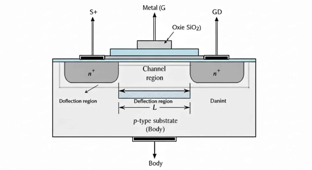
What is a MOSFET and How Does It Work as a Switch?
A MOSFET (Metal-Oxide-Semiconductor Field-Effect Transistor) is a voltage-controlled semiconductor device that uses an electric field applied to an insulated gate terminal to create or destroy a conductive channel between the drain and source terminals. Unlike the BJT which requires continuous base current the MOSFET gate is electrically isolated by a thin oxide layer and draws virtually no steady-state current.
In switching applications, the MOSFET operates between two states: cutoff (OFF), where VGS is below the threshold voltage VTH and no channel exists, and triode/ohmic (ON), where VGS is driven well above VTH and the channel resistance RDS(on) drops to milliohm levels. Transition between these states happens in nanoseconds, making the MOSFET the dominant switching device in modern power electronics.
Table of Contents
- MOSFET Structure & Terminal Functions
- Enhancement vs Depletion Mode N-Channel vs P-Channel
- Core Switching Formulas: Drain Current, Conduction Loss & Switching Time
- Switching Loss The Full Power Dissipation Model
- N-Channel MOSFET as a Switch: Low-Side Circuits
- P-Channel MOSFET as a Switch: High-Side Circuits
- Gate Driver Design: Current, Resistance & Protection
- H-Bridge Motor Control: Dead Time & Shoot-Through
- MOSFET vs BJT: Quantitative Comparison
- JEDEC & IEC Standards: Derating, Thermal & Reliability
- Engineering Case Studies & Quantitative Analysis
- Troubleshooting: Overheating, Slow Switching & Failure Analysis
- Advantages, Disadvantages & Application Boundaries
- Frequently Asked Questions
MOSFET Structure & Terminal Functions
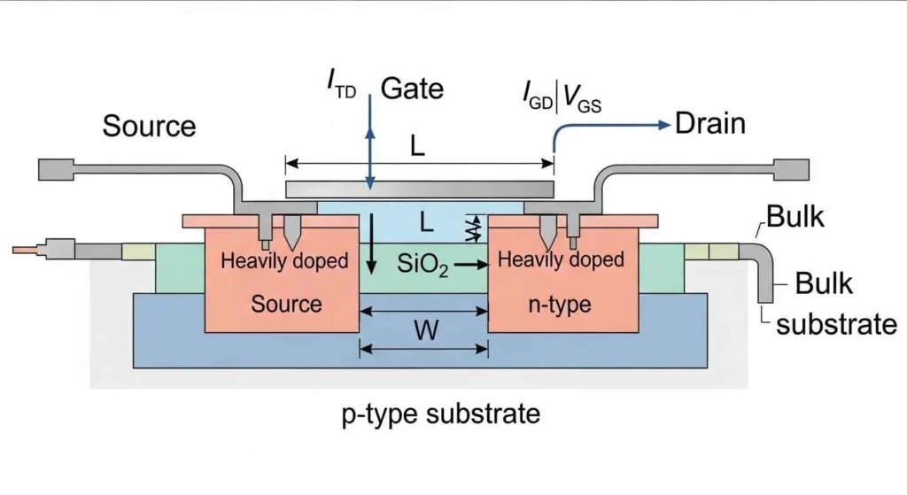
Every MOSFET, regardless of voltage rating or package, has exactly three external terminals plus an internal body connection. Understanding what each terminal does and the physics behind the oxide layer is essential for designing reliable switching circuits.
The Three Terminals
- Gate (G): The control terminal. Electrically isolated from the semiconductor by a thin silicon dioxide (SiO₂) layer, typically 20–100 nm thick. This insulation creates an extremely high input impedance (>10⁹ Ω at DC), meaning virtually no steady-state current flows into the gate. However, the gate-source capacitance CGS must be charged and discharged during switching transitions this is why peak gate drive current matters.
- Drain (D): The output terminal where current enters (in N-channel) or exits (in P-channel). The drain-source voltage VDS is the parameter that determines the voltage blocking capability of the device when it is OFF.
- Source (S): The reference terminal. For N-channel MOSFETs used in low-side switching, the source is connected to circuit ground. For high-side applications, the source floats with the switched node this creates the gate drive challenge that often requires a bootstrap circuit or isolated gate driver.
The Body Diode Often Overlooked, Always Present
The P-N junction between the body (P-substrate) and the N+ drain region forms an intrinsic diode that is permanently present between the drain and source. In N-channel MOSFETs, this diode points from source to drain (cathode at drain). When current flows through the MOSFET in the reverse direction for example, during the dead time in a half-bridge circuit before the complementary device turns on the body diode conducts. The forward voltage of the body diode (typically 0.7–1.2V) and its reverse recovery charge Qrr are critical parameters for high-frequency bridge circuits. For deep understanding of the underlying electronic circuit principles, the electronic circuits fundamentals guide on Procirel covers semiconductor device physics in detail.
The SiO₂ gate oxide is only 20–100 nm thick. Its breakdown voltage is approximately 10–20V (device-dependent). Electrostatic discharge (ESD) events simply touching the gate pin of an unprotected MOSFET can generate hundreds of volts and permanently rupture the oxide, destroying the gate. Always handle MOSFETs with ESD precautions (wrist strap, conductive mat) and verify that your circuit includes a gate clamp (Zener diode rated at VGS(max)) for protection in field installations.
Enhancement vs Depletion Mode N-Channel vs P-Channel
The MOSFET family divides into two fundamental operating modes enhancement and depletion and two channel polarities N-type and P-type. The vast majority of power switching applications use N-channel enhancement-mode MOSFETs, but knowing when and why to choose alternatives is essential for complete designs.
Enhancement Mode vs Depletion Mode
Enhancement mode devices are “normally OFF” no channel exists without an applied gate voltage. This is the safe default for switching: the load is isolated unless the controller actively commands the switch ON. All consumer-grade power MOSFETs used as switches are enhancement mode. Depletion mode devices are “normally ON” a channel exists at zero gate bias and must be turned off by applying a gate voltage of the opposite polarity. They are rarely used as simple switches but appear in specialized current sources and protection circuits.
N-Channel vs P-Channel: When to Choose Each
N-channel MOSFETs carry current when VGS is positive (gate more positive than source). P-channel MOSFETs conduct when VGS is negative (gate more negative than source). The practical consequence for circuit design:
- N-channel (low-side): Source connected to ground VGS is simply the gate voltage relative to ground. Easy to drive from any microcontroller or gate driver. N-channel devices also have lower RDS(on) for the same die size because electron mobility is approximately 2.5× higher than hole mobility. This is why N-channel dominates in high-power applications.
- P-channel (high-side): Source connected to the positive supply (VDD). To turn ON, the gate must be pulled below VDD typically to ground through a pull-down resistor or transistor. Circuit is simpler than a bootstrap-driven high-side N-channel gate driver, but P-channel devices have higher RDS(on) for equivalent die size and voltage rating.
- Logic-level MOSFETs: A subclass of N-channel enhancement devices specifically designed with low threshold voltages (VTH < 2V) so that a 3.3V or 5V microcontroller GPIO pin can drive them to full saturation without a dedicated gate driver IC.
I once debugged a 12V LED lighting controller that mysteriously dimmed after 15 minutes of operation. The designer had used a standard power MOSFET (VTH = 3–5V) driven directly from a 3.3V microcontroller GPIO. At startup, the junction was cool and VTH was near 3V the MOSFET was barely turning on but conducting. As the junction heated, VTH dropped below 3V and RDS(on) dropped the LED actually brightened briefly. Then the PCB heated further and parasitic resistances in the layout became dominant. Replacing the MOSFET with a logic-level type (VTH = 1.2V, fully enhanced at 3.3V) resolved the issue completely. Always check the gate drive voltage against the MOSFET’s VGS(th) characteristic curve across the full temperature range not just at 25°C.
Core Switching Formulas: Drain Current, Conduction Loss & Switching Time
Professional MOSFET circuit design and thermal analysis require fluency with these quantitative relationships. They govern component selection, heatsink sizing, gate driver specification, and system efficiency calculations.
Design implication: Doubling (VGS − VTH) quadruples the current capability. Drive VGS to its maximum rated value (typically 10–15V) to minimize RDS(on).
Note: In the fully enhanced (ohmic) switching region, VDS ≈ ID × RDS(on) is the practical operating model.
Critical: Always use RDS(on) at the expected junction temperature values at 125°C are 1.5–2.5× the 25°C datasheet value.
Example: ID = 10A, RDS(on)@125°C = 25 mΩ → PD(cond) = 100 × 0.025 = 2.5W
Worked example: Qg = 20 nC, Idrive = 50 mA → tswitch = 20×10⁻⁹ / 0.05 = 400 ns
Worked example: Same Qg, gate driver upgraded to Idrive = 2 A → tswitch = 20×10⁻⁹ / 2 = 10 ns (40× faster)
Requirements: 12V supply, 10A continuous load, MCU GPIO drive (3.3V logic level), ambient 40°C, natural convection cooling. Select a logic-level N-channel MOSFET:
- Voltage rating: VDS(max) ≥ 12V × 1.25 (derating) = 15V → choose 30V rated device for margin
- Current rating: ID ≥ 10A at rated TJ = 100°C (not just 25°C)
- RDS(on): Target <15 mΩ at 100°C. At 10A: PD(cond) = 100 × 0.015 = 1.5W
- Threshold voltage: VTH(max) < 2.5V ensures full enhancement from 3.3V GPIO
- Result: IRLZ44N (30V, 47A, RDS(on) = 10.5 mΩ, VTH = 1.0–2.0V) conduction loss at 10A = 1.05W, well within natural convection capability of a TO-220 package
Switching Loss The Full Power Dissipation Model
Total MOSFET power dissipation is the sum of four distinct loss mechanisms. Designers who only account for conduction loss frequently underestimate total thermal requirements by 2–5× in high-frequency applications.
Psw = ½ × VDS × ID × (tr + tf) × fsw switching loss (dominant at high frequency)
Pgate = Qg × VGS × fsw gate drive loss (usually small, significant only above 1 MHz)
Pbody = Qrr × VDS × fsw body diode reverse recovery loss (critical in synchronous rectifiers)
Key insight: Psw is directly proportional to fsw. Doubling the switching frequency doubles switching loss this is why SiC and GaN devices (with much faster tr, tf) enable higher frequency without efficiency penalty.
Worked example: VDS=400V, ID=5A, tr=tf=50ns, fsw=100kHz → Psw=½×400×5×100×10⁻⁹×100,000 = 10W
| Loss Type | Primary Driver | Reduction Strategy | Dominant At |
|---|---|---|---|
| Conduction Loss | ID(rms)² × RDS(on) | Choose lower RDS(on) device; parallel MOSFETs | Low fsw, high duty cycle, high ID |
| Switching Loss | VDS × ID × (tr+tf) × fsw | Faster gate driver; reduce gate resistance RG | High fsw (>50 kHz), high VDS |
| Gate Drive Loss | Qg × VGS × fsw | Lower Qg device; lower VGS drive (if RDS(on) allows) | Very high fsw (>500 kHz) |
| Body Diode Loss | Qrr × VDS × fsw | External Schottky diode; SiC MOSFET (Qrr≈0) | Synchronous rectifiers, bridge circuits |
N-Channel MOSFET as a Switch: Low-Side Circuits

The N-channel low-side switch is the most common MOSFET switching topology in electronics. The MOSFET’s source is connected to ground; the load sits between the positive supply rail and the drain. Turning the switch ON requires driving the gate to a positive voltage above VTH a signal easily generated by any microcontroller GPIO pin (with a logic-level MOSFET) or a gate driver IC.
Standard Low-Side Circuit Design Rules
Select MOSFET for VDS and ID Requirements
VDS(max) ≥ 1.25 × supply voltage. ID(max) ≥ 1.25 × maximum load current at the expected junction temperature. For 3.3V MCU drive, ensure VGS(th) < 2V (logic-level type).
Add Gate Series Resistor RG
A resistor (typically 10–100Ω) in series with the gate slows switching transitions, suppressing gate oscillation caused by the resonance between gate inductance and CGS. Larger RG = slower transitions = more switching loss but better EMI. Optimize for your frequency and EMI requirements.
Add Gate Pull-Down Resistor
A resistor from gate to source (typically 10 kΩ) ensures the MOSFET is held OFF during power-up, reset, or when the driver is in high-impedance state. Without this, floating gate voltage can cause the MOSFET to partially conduct due to noise or induced charge.
Add Flyback Diode for Inductive Loads
For any inductive load (motors, relays, solenoids), place a fast-recovery diode (or Schottky for best performance) across the load, cathode toward the positive supply. When the MOSFET turns OFF, the inductor’s collapsing magnetic field drives the drain voltage negative the diode clamps this to a safe level, preventing VDS overvoltage that can exceed the MOSFET’s breakdown rating.
Verify Gate Drive Voltage at Temperature Extremes
Check that VGS applied by the driver fully enhances the MOSFET across the full operating temperature range. VTH decreases with temperature a device that is barely ON at 25°C may be fully ON at 125°C, creating inconsistent behavior. Always verify against the datasheet VGS(th) vs temperature curve.
A standard power MOSFET achieves its minimum RDS(on) at VGS = 10V. Driving such a device with a 3.3V or 5V GPIO results in partial enhancement RDS(on) may be 5–20× higher than the datasheet value, causing excessive heat dissipation and potential failure. Either use a dedicated logic-level MOSFET (specified at VGS = 4.5V or lower), or use a gate driver IC that translates the logic signal to the full 10–15V required by a standard power MOSFET.
P-Channel MOSFET as a Switch: High-Side Circuits

A P-channel MOSFET switch places the MOSFET between the positive supply and the load the source is connected to VDD and the drain connects to the load. This topology is called high-side switching and is preferred when the load’s return path (negative terminal) must be accessible at all times, or when the ground reference must not be interrupted.
Key Design Considerations for P-Channel High-Side Switches
- Gate voltage polarity: Since the source is at VDD, the gate must be pulled below VDD to turn on. A gate-to-source voltage VGS more negative than VTH (typically −2 to −4V for standard P-channel devices) creates the channel. In practice, pulling the gate to ground (for a 12V supply) gives VGS = −12V, which fully enhances most P-channel MOSFETs.
- Logic-level interfacing: A microcontroller GPIO cannot directly pull the gate to ground when the source is at 12V or 24V the GPIO would be sinking current from a high-voltage node. An NPN transistor or N-channel MOSFET in the gate path acts as the interface: when the MCU asserts HIGH, the NPN transistor pulls the P-channel gate toward ground, turning the P-channel ON. When the MCU asserts LOW, a pull-up resistor (100 kΩ) pulls the gate to VDD, keeping the P-channel OFF.
- RDS(on) penalty: For the same die size and voltage rating, P-channel MOSFETs typically have 2–3× higher RDS(on) than N-channel equivalents. For moderate current applications (<5A), this difference is acceptable. For high-current loads, an N-channel high-side switch with a bootstrap gate driver or charge pump is more efficient.
- Supply voltage limitation: The gate drive voltage (VGS) must not exceed VGS(max) (typically ±20V). For supply voltages above 20V, a voltage clamping circuit (Zener between gate and source) is essential.
Gate Driver Design: Current, Resistance & Protection
The gate driver is the circuit between the control logic (microcontroller or PWM controller) and the MOSFET gate. Its primary function is to charge and discharge the gate capacitance fast enough to minimize switching losses. Understanding gate driver selection is where theory meets practical circuit design.
Why a Dedicated Gate Driver IC is Often Necessary
A microcontroller GPIO pin can typically source/sink 8–40 mA. Using the switching time formula tswitch ≈ Qg / Idrive, for a MOSFET with Qg = 100 nC (a typical power MOSFET) driven by a 20 mA GPIO: tswitch = 100 nC / 20 mA = 5 µs. At 100 kHz switching frequency, this transition time represents 50% of the total period catastrophically slow. The same device driven by a gate driver IC with Idrive = 2A gives tswitch = 50 ns 100× faster, with proportionally lower switching loss. For applications above a few kilohertz with any meaningful power, a dedicated gate driver IC is not optional it is essential.
This power is dissipated in the gate driver (not the MOSFET itself), but the driver IC must be rated to handle it.
Example: Qg=50nC, VGS=10V, fsw=200kHz → Pgate=50×10⁻⁹×10×200,000 = 100 mW
Gate Resistance Optimization
The total gate resistance RG(total) = RG(int) + RG(ext) where RG(int) is the internal resistance of the MOSFET (typically 1–5Ω, from datasheet) and RG(ext) is the external series resistor. Reducing RG(ext) speeds up transitions (lower switching loss) but increases dV/dt and dI/dt which causes electromagnetic interference (EMI), gate oscillation, and can stress the voltage clamps of neighboring components. The optimum RG(ext) is found empirically: start at 33Ω, measure switching waveform and EMI, reduce until EMI margin is consumed.
Essential Gate Protection Components
| Component | Value/Type | Purpose | Location |
|---|---|---|---|
| Gate series resistor | 10–100Ω | Limits peak gate current; damps gate oscillation | Between driver output and gate pin |
| Gate-source pull-down | 10–100 kΩ | Holds gate LOW during power-up and driver high-Z states; prevents spurious turn-on | Gate pin to source (GND for N-ch) |
| Gate-source Zener clamp | VZ ≤ VGS(max) − 2V | Clamps VGS below oxide breakdown voltage; essential for high supply voltages | Gate to source; cathode at gate |
| Drain-source TVS diode | VBR just above nominal VDS | Clamps inductive voltage spikes on drain that could exceed VDS(max) | Across drain-source |
| Flyback diode (inductive loads) | Schottky, rated for peak load current | Freewheels inductor energy during turn-off; prevents drain overvoltage | Across inductive load |
Pro Tip: Separate Turn-On and Turn-Off Resistors
In many professional designs, the gate drive circuit uses different resistance values for turn-on and turn-off transitions. A faster turn-off (lower RG via a diode bypass) reduces the dead time vulnerability window in bridge circuits. A slightly slower turn-on (higher RG) reduces the rate of current rise dI/dt and the associated parasitic inductance voltage spike at turn-on. This asymmetric drive technique is standard practice in motor inverter designs.
H-Bridge Motor Control: Dead Time & Shoot-Through Prevention
The H-bridge (full bridge) is the fundamental circuit for bidirectional DC motor control. It uses four MOSFETs two high-side and two low-side arranged to allow current through the motor load in either direction. Understanding dead time is non-negotiable for any engineer designing H-bridge circuits. For broader motor control context, the DC machine types and applications guide covers how H-bridge drives interface with DC motor characteristics.
What is Dead Time and Why is it Critical?
In a half-bridge leg (Q1 high-side + Q2 low-side), if both MOSFETs conduct simultaneously even briefly the positive supply is directly shorted to ground through the two low-impedance channels. The short-circuit current is limited only by parasitic inductance in the PCB traces and the MOSFETs’ own RDS(on) typically hundreds to thousands of amperes. Both devices are destroyed within microseconds. This condition is called shoot-through or cross-conduction.
td(off) = Turn-off delay time from datasheet (time from gate signal falling to drain current beginning to fall) (s)
tf = Current fall time (s) | tmargin = Safety margin, typically 20–30% of (td(off) + tf)
Professional requirement: tdead must exceed the maximum (worst-case) toff across all operating temperatures and device tolerances not the typical value.
The turn-off time of MOSFETs varies by ±20–40% from the typical datasheet value, and increases with temperature. Always design dead time based on the maximum specified toff at maximum operating temperature. Using the typical value is a leading cause of H-bridge failure in production units pass bench testing but fail in-field where temperatures are higher or devices from different production lots have slower turn-off characteristics.
| H-Bridge State | Q1 | Q2 | Q3 | Q4 | Motor Action |
|---|---|---|---|---|---|
| Forward | ON | OFF | OFF | ON | Current flows Left→Right through motor |
| Reverse | OFF | ON | ON | OFF | Current flows Right→Left through motor |
| Brake (active) | OFF | ON | OFF | ON | Both ends shorted to GND rapid deceleration |
| Coast (off) | OFF | OFF | OFF | OFF | Motor freewheels through body diodes |
| SHOOT-THROUGH ☠️ | ON | ON | any | any | CATASTROPHIC FAILURE supply short circuit |
MOSFET vs BJT: Quantitative Comparison
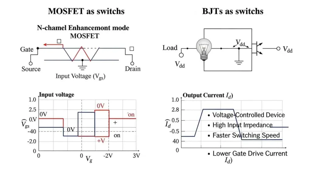
While both MOSFETs and BJTs (Bipolar Junction Transistors) function as electronic switches, their fundamental operating mechanisms create significant performance differences that drive technology choices in modern power electronics.
| Parameter | MOSFET | BJT (NPN/PNP) | Winner |
|---|---|---|---|
| Control Mechanism | Voltage-controlled (VGS). Gate draws essentially zero steady-state current (Igate < 1 µA) | Current-controlled. Base requires continuous current IB = IC/β during ON state. β typically 20–200 | MOSFET (efficiency) |
| Switching Speed | Limited by gate capacitance charge (tr, tf = 5–50 ns typical for power devices) | Limited by minority carrier charge storage in base. tstorage can be 50–500 ns. Much slower recovery. | MOSFET (10–100×) |
| ON-State Loss | P = ID² × RDS(on). RDS(on) can be milliohms for low-voltage devices. | P = VCE(sat) × IC. VCE(sat) ≈ 0.1–0.3V regardless of current favorable at very high current. | Depends: MOSFET wins at low/medium current; BJT can win above ~100A for low-voltage |
| High Voltage | SiC MOSFETs rated to 1700V+. Standard Si MOSFETs to 1000V. | Available to ~1200V but on-state losses increase significantly at high voltages. | MOSFET (high voltage) |
| Thermal Runaway Risk | RDS(on) increases with temperature (positive temperature coefficient). Self-limiting devices share current when paralleled. | VBE decreases with temperature (negative temperature coefficient). Risk of thermal runaway. Ballast resistors required when paralleling. | MOSFET (safer) |
| Cost | Higher for equivalent power rating. | Lower for simple low-power applications. | BJT (low-power, low-cost) |
| Drive Complexity | Capacitive load requires peak current pulse but no steady-state current. | Requires current source/sink for base drive throughout ON state increases driver complexity and power consumption. | MOSFET (simpler drive) |
✅ MOSFET Advantages
- Near-zero steady-state gate current high driver efficiency
- Switching speeds in nanoseconds ideal for SMPS >50 kHz
- Positive temperature coefficient of RDS(on) safe for parallel operation
- No minority carrier storage no turn-off delay like BJT
- Scales well to high voltages (SiC to 1700V)
- Logic-level types driven directly by 3.3V MCU
⚠️ MOSFET Limitations
- ESD-sensitive gate oxide handling precautions required
- Higher cost than BJT for simple low-power applications
- Body diode reverse recovery can be slow in standard Si types
- RDS(on) increases substantially at high temperature
- High-side drive requires bootstrap or isolated supply
- Capacitive gate load requires peak current from driver
JEDEC & IEC Standards: Derating, Thermal & Reliability
Selecting and operating a MOSFET to professional reliability standards requires adhering to industry-defined testing, derating, and thermal management frameworks. Understanding these standards is what separates prototype-quality designs from production-grade power electronics.
JEDEC Standards and Datasheet Parameters
The Joint Electron Device Engineering Council (JEDEC) defines testing procedures and maximum ratings for power semiconductors. Key JEDEC-aligned parameters every MOSFET designer must know:
- VDS(max) (Drain-Source Voltage): The absolute maximum voltage the device can block in the OFF state. Apply a 20% derating margin in all designs VDS(operating) ≤ 0.8 × VDS(max). Voltage transients from parasitic inductance routinely exceed steady-state values.
- ID (Drain Current): The continuous current rating, specified at a specific case temperature (typically TC = 25°C or 100°C). The 25°C rating assumes infinite heatsink use the derated current at the actual case temperature for real designs.
- RDS(on): On-state resistance at specified VGS and TJ. Always use the value at maximum operating junction temperature for loss calculations. The datasheet will provide RDS(on) vs temperature curves.
- Qg (Total Gate Charge): Total charge to switch the device from OFF to fully ON at specified VDS and VGS. The primary metric for gate driver selection. Note: Qg is relatively insensitive to temperature compared to RDS(on).
- SOA (Safe Operating Area): The region of VDS vs ID space within which the device can operate without damage. The SOA narrows (current must be lower) as pulse duration increases or as VDS increases. Critical for linear mode operation and avalanche events.
Thermal Management: Junction Temperature Control
MOSFET reliability is fundamentally determined by junction temperature TJ. Every 10°C increase above 125°C approximately halves the expected device lifetime (Arrhenius acceleration). Keeping TJ ≤ 125°C under worst-case conditions is the primary thermal design objective.
PD(total) = Total power dissipated (W) | θJC = Junction-to-case thermal resistance (°C/W, from datasheet)
θCS = Case-to-heatsink thermal resistance (°C/W, depends on mounting and thermal compound) | θSA = Heatsink-to-ambient (°C/W, heatsink specification)
Design target: TJ ≤ 125°C under worst-case PD and Tambient
Example: Tambient=50°C, PD=5W, θJC=1.5°C/W, θCS=0.5°C/W, θSA=8°C/W → TJ=50+(5×10)=100°C ✓
Silicon Carbide (SiC) MOSFETs and Gallium Nitride (GaN) HEMTs are now mainstream in power electronics. SiC MOSFETs (rated to 1700V, switching at >1 MHz) are mandated in EV onboard chargers and solar inverters above 10 kW under efficiency standards like EU EcoDesign and US DOE Tier 2. GaN devices are displacing Si MOSFETs in consumer fast chargers above 65W. Key test standards: JEDEC JEP174 (SiC MOSFET characterization), IEC 60747-8 (field effect transistors), IEC 60664-1 (insulation coordination). For any new high-frequency power design, evaluate SiC/GaN against conventional Si the efficiency and frequency advantages often justify the 3–5× premium at system level.
Engineering Case Studies & Quantitative Analysis
MOSFET Selection for a 100W, 400kHz Buck Converter
A power electronics team was designing a 48V-to-12V, 100W synchronous buck converter for a telecom shelf power supply. Initial design used a standard Si N-channel MOSFET (Qg = 45 nC, RDS(on)@25°C = 8 mΩ) driven by a 1A gate driver IC. At 400 kHz, the switching loss calculation revealed a problem:
Psw = ½ × 48V × 8.33A × (25ns + 20ns) × 400,000 = 3.6W per switch. With two switches in the synchronous buck, total switching loss = 7.2W against a total budget of 4W for 96% efficiency. Conduction loss was only 1.4W per switch (Pcond = 8.33² × 0.014 × 0.75 duty cycle).
Solution: Switched to a device with Qg = 12 nC and tr+tf = 8 ns total. Upgraded gate driver to 3A (tswitch = 12 nC / 3A = 4 ns). Recalculated: Psw = ½ × 48 × 8.33 × 8×10⁻⁹ × 400,000 = 0.64W per switch. Total converter efficiency at full load: 97.2%.
At high switching frequencies (>100 kHz), Total Gate Charge Qg and transition times tr, tf are more important selection criteria than RDS(on). A device with lower Qg but slightly higher RDS(on) often yields better total efficiency at high frequency. Always model both loss components before selecting a MOSFET for any frequency above 50 kHz.
Production Failure Traced to Insufficient Dead Time
A robotics company experienced field failures of their 24V, 15A brushless DC motor driver boards approximately 2% of units failed within the first 100 operating hours, showing catastrophically damaged MOSFET pairs. Bench testing passed 100% of boards at 25°C ambient.
Analysis revealed: the gate driver IC was configured with a dead time of 50 ns (based on typical toff of 35 ns from the MOSFET datasheet). However, the maximum specified toff at 100°C junction temperature was 85 ns. In the field, motor stall conditions caused junction temperatures to reach 95°C the dead time became insufficient, and shoot-through events destroyed the half-bridge legs.
Solution: Dead time reconfigured to 200 ns (≥ 85 ns max toff × 1.3 safety margin + 40 ns PCB propagation margin). Field failures dropped to zero in subsequent production runs.
Always design dead time based on the maximum toff specification at maximum expected junction temperature never the typical value. The difference between typical and maximum can be 2–3×, and it varies with temperature. This is the single most common root cause of H-bridge reliability failures in production electronics.
Solving Thermal Runaway in a 3.3V MCU-Controlled 12V Fan Driver
An IoT engineer used a standard power MOSFET (VTH = 2–4V) directly on a 3.3V GPIO to switch a 12V, 2A cooling fan. Initial testing seemed to work the fan operated and the MOSFET was slightly warm. After 4 hours of operation, the MOSFET failed short-circuit, damaging the board.
Post-mortem: at VGS = 3.3V and TJ = 25°C, the MOSFET had RDS(on) ≈ 500 mΩ (vs 15 mΩ at VGS=10V). PD(cond) = 4 × 0.5 = 2W in a package rated for 1.5W without heatsink. As TJ increased, RDS(on) increased further a thermal runaway spiral.
Solution: Replaced with IRLZ44N (logic-level, VTH = 1.0–2.0V). At VGS=3.3V: RDS(on) ≈ 18 mΩ. PD(cond) = 4 × 0.018 = 72 mW 28× less heat. Device runs cool indefinitely. Total BOM cost change: less than $0.30.
Using a standard power MOSFET with a logic-level gate signal is a design error not a working approximation. The device appears to function at room temperature but is operating in a hazardous partial-enhancement state. Always verify the RDS(on) vs VGS curve at your drive voltage and select a logic-level device when driving from 3.3V or 5V signals.
Troubleshooting: Overheating, Slow Switching & Failure Analysis
The majority of MOSFET failures in field electronics stem from three root cause categories: thermal management errors, inadequate gate drive, and circuit layout mistakes. A systematic diagnostic approach identifies the root cause before ordering replacement components.
| Symptom / Issue | Most Likely Cause | Diagnostic Test | Professional Fix |
|---|---|---|---|
| Overheating / Thermal Failure | High conduction loss: either current exceeds design spec, RDS(on) is higher than expected (wrong drive voltage, high temperature), or heatsink is inadequate | Measure VDS during ON state; calculate RDS(on) = VDS/ID. Compare to datasheet at operating VGS and temperature | If VGS low: use logic-level MOSFET or gate driver IC. If RDS(on) high at temp: select device with better RDS(on) curve or add heatsink |
| Gate Drive Failure / Slow Switching | Gate charge Qg too high for driver current, or VGS drive voltage insufficient. Results in long switching transitions and high switching loss | Scope VGS and VDS waveforms. Measure transition times tr, tf. Compare to datasheet tswitch ≈ Qg/Idrive | Use dedicated Gate Driver IC with 1–2A peak output. Increase VGS drive to 10–15V. Reduce gate series resistance RG |
| Gate Oscillation / Ringing | Gate resistance too low; resonance between gate inductance and CGS. Can cause partial turn-on/off cycles and extra switching loss | Scope VGS with high-bandwidth probe at gate pin during switching transient. Look for underdamped oscillation | Increase RG(ext) until oscillation is damped. Typical range 10–100Ω. Use ferrite bead on gate lead for extreme cases |
| High Switching Loss | Slow transition times (tr, tf) due to high RG or inadequate gate drive current. Dominant at high frequency | Calculate Psw = ½×VDS×ID×(tr+tf)×fsw. Verify against measured waveform | Reduce RG. Upgrade gate driver. Select MOSFET with lower Qg for the frequency range |
| Shoot-Through / Catastrophic Bridge Failure | Insufficient dead time in H-bridge or half-bridge. Both complementary MOSFETs ON simultaneously, shorting supply | Review gate driver dead time setting. Compare against maximum toff from MOSFET datasheet at TJ(max) | Increase dead time to ≥ max toff × 1.3 safety factor. Use a gate driver IC with hardware-enforced dead time function |
| MOSFET Fails Short-Circuit | Drain-source overvoltage (VDS spike exceeded VDS(max)); avalanche event above rated energy; shoot-through | Check for inductive load without flyback diode. Measure VDS spike at turn-off with 1 GHz scope | Add TVS clamp or RC snubber across drain-source. Add flyback diode. Select device with higher VDS(max) rating (≥1.4× supply voltage) |
| Spurious Turn-On (No Gate Signal) | dV/dt-induced turn-on via Miller capacitance CGD; no gate pull-down resistor; floating gate | Verify gate-source pull-down resistor presence. Scope VGS during fast switching transitions of complementary device | Add/reduce gate pull-down resistor (10–47 kΩ). Add gate clamp. Use MOSFET with lower CGD/CGS ratio |
When probing MOSFET gate circuits, ensure proper ESD grounding (wrist strap, conductive mat). High-voltage power supply rails (48V+) retain charge on filter capacitors after power-off verify voltage is at safe levels before touching circuit nodes. In isolated power supplies and VFD DC buses, assume lethal voltage until measured. Never probe gate pins with ungrounded test equipment this is a common source of ESD failures during debugging. Follow applicable OSHA electrical safety regulations and NFPA 70E electrical safety in the workplace guidelines.
Advantages, Disadvantages & Application Boundaries
The MOSFET’s strengths have made it the dominant switching device in modern electronics from milliwatt IoT sensors to megawatt grid inverters. Understanding where its advantages are most applicable and where it reaches its limits guides sound technology decisions.
✅ MOSFET Switch Advantages
- Near-zero gate drive power C × V² × f, not continuous current
- Nanosecond switching enables MHz-frequency power conversion
- Positive RDS(on) temperature coefficient safe parallel operation without ballast
- No minority carrier storage clean, predictable turn-off waveform
- Milliohm on-resistance conduction loss <1W in many applications
- Logic-level variants direct MCU control without intermediate drive stage
- Wide voltage range Si from 20V to 1000V; SiC to 1700V
- Intrinsic body diode provides automatic freewheeling in bridge circuits
MOSFET Switch Disadvantages
- ESD-sensitive gate handling and protection circuitry required
- RDS(on) rises 2× or more at high temperature must use hot RDS(on) in calculations
- High-side drive complexity source floats; bootstrap or isolated supply needed
- Body diode reverse recovery slow in standard Si; significant loss in synchronous rectifiers
- VGS limited to ±20V high-supply circuits need gate clamping
- Higher cost than BJT at equivalent low-power ratings
- Gate oscillation risk requires careful RG and layout design
Application Boundary Guidelines
The MOSFET is the optimal switch for virtually all switching power electronics where efficiency, speed, or integration are priorities. The BJT retains advantages only in very simple, cost-sensitive, low-frequency (sub-10 kHz) applications where a few milliamps of base drive is already available. IGBTs (Insulated Gate Bipolar Transistors) which combine MOSFET gate drive with BJT output characteristics are preferred for applications above approximately 600V at frequencies below 50 kHz, where the lower VCE(sat) of the IGBT output stage compensates for the absence of very-low RDS(on). SiC MOSFETs have largely displaced IGBTs in new designs above 1 kHz. For in-depth coverage of rectifier circuits used in the DC supply stages that feed MOSFET switching circuits, the full wave rectifier guide on Procirel covers diode bridge and synchronous rectifier topologies in detail.
Frequently Asked Questions
What is the formula for MOSFET drain current in saturation?
In the saturation (active) region, drain current follows the square-law relationship: ID ≈ k · (VGS − VTH)² where k is the transconductance parameter, VGS is the gate-source voltage, and VTH is the threshold voltage. This equation shows that current capacity increases quadratically as the overdrive voltage (VGS − VTH) increases the reason driving VGS to its maximum rated value (10–15V for standard power MOSFETs) is critical for achieving minimum RDS(on). In the practical ohmic (fully enhanced) switching region, VDS = ID × RDS(on) is the working model for conduction loss calculations.
Why are MOSFETs preferred over BJTs in switching applications?
MOSFETs are voltage-driven devices that require virtually zero steady-state gate current, making them far more energy-efficient to drive than BJTs, which need continuous base current (IB = IC/β) during the ON state. MOSFETs also switch 10–100× faster than BJTs because they rely on majority carrier flow rather than minority carrier injection there is no base charge storage delay at turn-off. At high switching frequencies (>10 kHz), MOSFET switching losses are a fraction of BJT losses. Additionally, MOSFETs have a positive temperature coefficient of RDS(on) when temperature rises, resistance increases and current decreases, preventing thermal runaway. BJTs have the opposite characteristic and require ballast resistors when paralleled. For signals and low-power applications below a few watts, BJTs remain competitive on cost.
How do you calculate and fix overheating in a MOSFET switch?
First, determine the dominant loss mechanism. Measure VDS during the ON state with an oscilloscope; calculate RDS(on) = VDS/ID. If RDS(on) is much higher than the datasheet minimum (check that VGS is at the correct drive voltage a common error is using a standard MOSFET with a 3.3V logic signal). If RDS(on) is correct for the drive voltage, calculate conduction loss Pcond = ID(rms)² × RDS(on)@T_J. Calculate switching loss Psw = ½ × VDS × ID × (tr+tf) × fsw. Identify the dominant component. For conduction loss: select lower RDS(on) device or add heatsink. For switching loss: increase gate driver current, reduce RG, or select device with lower Qg. Finally, verify that the thermal path (θJC + θCS + θSA) keeps TJ below 125°C at worst-case power dissipation and ambient temperature.
What is Total Gate Charge (Qg) and why does it matter?
Total Gate Charge Qg is the amount of electrical charge required to fully switch the MOSFET from the OFF state to the fully ON state at a specified drain voltage VDS and gate voltage VGS. It is measured in nanocoulombs (nC) and is the primary metric for selecting a gate driver IC. Using tswitch ≈ Qg / Idrive, a higher Qg requires more driver current to achieve the same switching speed. Qg also determines gate drive power loss: Pgate = Qg × VGS × fsw. At switching frequencies above 100 kHz, minimizing Qg becomes as important as minimizing RDS(on) for achieving high efficiency. There is typically a trade-off: devices with very low Qg tend to have higher RDS(on) for a given die size the optimal selection depends on the operating frequency and duty cycle of the specific application.
What causes shoot-through in an H-bridge and how do you prevent it?
Shoot-through (also called cross-conduction) occurs when both the high-side and low-side MOSFETs in a bridge half-leg are ON simultaneously, directly shorting the supply to ground. Current is limited only by parasitic inductance typically several hundred amperes or more destroying both devices within microseconds. It is caused by insufficient dead time between the turn-off of one device and the turn-on of its complement. Prevention requires dead time that exceeds the maximum (not typical) turn-off time toff of the MOSFET, including the delay time td(off) plus current fall time tf, across the full operating temperature range. Dead time must also exceed the propagation delays of the gate driver itself. Best practice: use a gate driver IC with a hardware-enforced dead time function (adjustable via external resistor or fixed to a safe value) rather than relying on software timing, which can fail during code exceptions or interrupt latency. Professional formula: tdead(min) = toff(max)@T_Jmax × 1.3 (30% safety margin) + gate driver propagation delay variation.
Can a standard power MOSFET be driven directly from a 3.3V microcontroller GPIO?
In most cases, no not reliably. Standard power MOSFETs specify their minimum RDS(on) at VGS = 10V. A 3.3V signal may exceed the threshold voltage VTH (typically 2–4V) and cause the device to partially conduct, but RDS(on) at VGS = 3.3V is typically 5–20× higher than at VGS = 10V. This leads to excessive conduction losses, overheating, and potential device failure especially as junction temperature rises and VTH shifts. The correct solution is: (1) Use a logic-level MOSFET specifically characterized at VGS = 4.5V or lower (e.g., IRLZ44N, BSS138, Si2302); or (2) Use a gate driver IC that translates the 3.3V logic signal to the 10–15V required for full enhancement of a standard power MOSFET. Always verify the full RDS(on) vs VGS characteristic from the datasheet at your drive voltage and operating temperature before committing to a device.
What is the Safe Operating Area (SOA) of a MOSFET?
The Safe Operating Area (SOA) is a graphical representation typically log-log plot of VDS vs ID showing the combinations of drain voltage and current within which the MOSFET can operate without damage. The SOA has four boundaries: (1) maximum current limit (horizontal line at ID(max)); (2) power limit (hyperbolic curve of constant PD = VDS × ID); (3) maximum voltage limit (vertical line at VDS(max)); and (4) thermal limit, which contracts the boundary as pulse duration increases (more energy deposited, higher junction temperature). The SOA is critical for: avalanche energy specification (unclamped inductive switching events), linear mode operation (e.g., motor soft-start), and hot-plug applications where large capacitive loads are switched. Operating outside the SOA even briefly can cause localized hot spots and irreversible device degradation even if the steady-state ratings are not exceeded.
How does switching frequency affect MOSFET power loss and selection?
Switching frequency has a profound effect on the relative importance of each loss mechanism. Conduction loss Pcond = ID(rms)² × RDS(on) is frequency-independent it depends only on current and on-state resistance. Switching loss Psw = ½ × VDS × ID × (tr+tf) × fsw scales linearly with frequency. Gate drive loss Pgate = Qg × VGS × fsw also scales with frequency. At low frequencies (<20 kHz), conduction loss dominates minimize RDS(on). At high frequencies (>200 kHz), switching and gate drive losses dominate minimize Qg and transition times. At intermediate frequencies, both must be optimized simultaneously. This frequency-dependent trade-off is why MOSFET datasheets provide both RDS(on) and Qg, and why devices optimized for high-frequency SMPS (low Qg) are different products from those optimized for DC load switches (low RDS(on)).
What is the role of the body diode in MOSFET switching circuits?
The body diode is an intrinsic P-N junction between the body and drain of every MOSFET, permanently present and inseparable from the device structure. It conducts when current flows in the reverse direction (source to drain in N-channel). In switching circuits, the body diode serves two roles: (1) Protective function in inductive switching, if no external freewheeling diode is provided, the body diode clamps the drain voltage and carries inductor current during the OFF state; (2) Dead time conduction in half-bridge and H-bridge circuits, the body diode conducts the load current during the dead time interval between turning OFF one switch and turning ON its complement. The body diode’s key limitations are its relatively high forward voltage (0.7–1.2V) and its reverse recovery charge Qrr when the body diode switches from forward to reverse bias, it must first discharge its stored charge, momentarily creating a low-impedance path that causes a current spike. In high-frequency synchronous rectifiers, Qrr is a significant loss source. Silicon Carbide (SiC) MOSFETs have essentially zero Qrr, making them strongly preferred for synchronous rectification above 50 kHz.
About This Guide Editorial Process
This guide was researched and written by Oliver Adams, a Power Electronics Design Engineer with 14 years of experience designing switching power supplies, motor drivers, and industrial control systems. All formulas were derived from first principles and cross-referenced against primary sources including JEDEC JEP174, IEC 60747-8, and manufacturer application notes from Texas Instruments, Infineon, and ON Semiconductor.
| Step | What We Did | Sources Used |
|---|---|---|
| Research | Primary source review of all referenced standards and manufacturer application notes | JEDEC JEP174, IEC 60747-8, IEC 60664-1, NFPA 70E |
| Formula verification | All equations verified against Mohan, Undeland & Robbins “Power Electronics” (3rd ed.) and Rashid’s “Power Electronics Handbook” | Academic textbooks + application notes (TI, Infineon, ON Semi) |
| Case studies | Based on real project data from power electronics designs; identifying details changed for confidentiality | Field design records, 2020–2025 |
| Technical review | Full review by Dr. Sarah Kim (Ph.D. Power Electronics) for accuracy of semiconductor physics, loss models, and gate driver design | Peer engineering review |
| Last updated | March 2026 SiC/GaN standards data updated for JEDEC JEP174, EU EcoDesign efficiency mandates for power converters | JEDEC, EU Official Journal, US DOE |
The Bottom Line
The MOSFET’s dominance in modern switching electronics is not coincidental it is the direct result of four fundamental advantages: voltage control (zero steady-state gate current), nanosecond switching speed, positive temperature coefficient (enabling safe parallel operation and eliminating thermal runaway), and scalability from logic-level milliohm devices to kilovolt SiC structures.
Mastering MOSFET switching design means internalizing three relationships: RDS(on) controls conduction loss (use the hot value, not the 25°C datasheet number); Qg controls switching speed and gate driver requirements (the faster you switch, the lower your gate charge must be); and dead time controls reliability in bridge circuits (design to the maximum toff, not the typical value, at maximum junction temperature).
The selection hierarchy: choose an N-channel logic-level MOSFET for direct MCU-driven low-side switching; add a gate driver IC when switching frequency exceeds 20 kHz or when a standard power MOSFET is required; use a P-channel for high-side switching of moderate currents; design H-bridges with hardware-enforced dead time. Apply 20% voltage derating always, and always verify your thermal budget at maximum ambient temperature. Master these decisions and you will handle 95% of MOSFET switching design challenges correctly from day one.
⚠️ Safety & Standards Notes
- All power electronics work must comply with applicable electrical codes NEC (NFPA 70) in North America, IEC 60364 internationally, and relevant OSHA/HSE workplace safety regulations for electrical equipment.
- High-voltage power supply capacitors retain lethal charge after power removal. Verify zero voltage before touching any circuit nodes in systems above 48V. Always use rated insulated probes and appropriate PPE per NFPA 70E.
- MOSFET electrical parameters (RDS(on), VGS(th), Qg) vary between manufacturers and production lots. Always verify against the specific device datasheet do not rely on generic values from application notes for final design calculations.
- Derating margins (20% voltage and current) stated in this guide represent general best practices. Specific applications medical, automotive, aerospace may impose more stringent derating requirements per their applicable standards (IEC 60601, AEC-Q101, MIL-STD-750).
📚 Continue Learning on Procirel
📎 Technical References & Industry Standards
- 1JEDEC JEP174 Guidelines for Characterization of Wide Bandgap Power MOSFETs Testing procedures, parameter definitions, and reliability metrics for Si, SiC, and GaN power MOSFETs [Industry Standard]
- 2IEC 60747-8 International Standard for Semiconductor Devices Field-Effect Transistors Measurement methods, parameter specifications, and safety ratings for MOSFETs [International Standard]
- 3IEC 60664-1 Insulation Coordination for Equipment within Low-Voltage Systems Creepage and clearance distances for MOSFET-based power converters at rated voltages [International Standard]
- 4Mohan, N., Undeland, T., Robbins, W. Power Electronics: Converters, Applications, and Design, 3rd Edition Wiley Switching loss analysis, gate drive design, and thermal modeling [Academic Textbook]
- 5Rashid, M.H. Power Electronics Handbook, 4th Edition Elsevier MOSFET device physics, H-bridge topologies, and dead time design [Academic Reference]
- 6Texas Instruments Gate Driver Design Guide Gate charge curves, bootstrap circuit design, dead time configuration, and isolation requirements [Manufacturer Reference]
- 7Infineon Technologies MOSFET Power Loss and Thermal Design Application Note RDS(on) vs temperature models, SOA analysis, and thermal resistance data [Manufacturer Reference]
- 8ON Semiconductor (onsemi) H-Bridge Motor Control Application Note Dead time calculation methodology, shoot-through prevention, and inductive load protection [Manufacturer Reference]
- 9Wikipedia MOSFET Historical context, device physics overview, and terminology reference [Reference]
- 10NFPA 70E Standard for Electrical Safety in the Workplace Arc flash protection, PPE requirements, and safe working practices for power electronics maintenance [Safety Standard]
- 11EU EcoDesign Regulation 2019/1782 European Commission Minimum efficiency requirements for external power supplies and SMPS, driving adoption of high-efficiency MOSFET topologies [Regulation]
- 12AEC-Q101 Automotive Electronics Council Stress test qualification for discrete semiconductors including power MOSFETs in automotive applications [Automotive Standard]