Introduction to MOSFET as a Switch
The MOSFET as a switch is the cornerstone of modern power electronics, enabling efficient control over high-power systems. Short for Metal Oxide Semiconductor Field Effect Transistor, the MOSFET acts as a voltage-controlled gatekeeper, directing or blocking large currents based on a minuscule input signal. This guide moves beyond simple definitions to provide the formulas, quantitative analysis, and industry standards required to design reliable circuits for applications ranging from high-frequency Switched-Mode Power Supplies (SMPS) to precise motor control.
What is a MOSFET?
A MOSFET is a type of transistor that uses an electric field applied to the insulated Gate terminal to create a conductive channel between the Drain and Source. This architecture makes it voltage-controlled, drawing virtually no steady-state input current. Its primary advantage in switching applications is its exceptionally low On-State Resistance RDS(on), which minimizes power loss as heat. In essence, the MOSFET operates as an ideal, loss-less, high-speed switch a crucial component for energy-efficient power conversion.
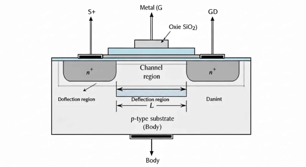
How Does a MOSFET Work as a Switch?

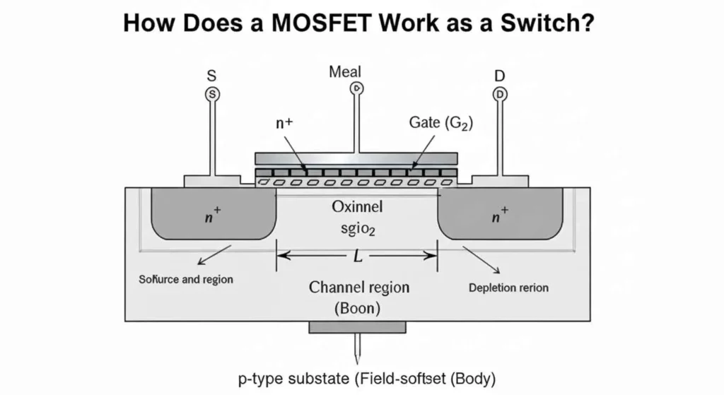
The MOSFET working principle revolves around applying voltage to the gate to create or disrupt a conductive channel. For an enhancement mode MOSFET, the most common type used as a switch, no channel exists until you apply a positive gate voltage for an N-channel or negative for a P-channel.
When the gate voltage exceeds the threshold, known as Vgs threshold, electrons or holes form a channel, allowing current to flow. In the cutoff region, with gate voltage below the threshold, the MOSFET acts like an open switch, blocking current. In the saturation region, it behaves like a closed switch, letting current pass with minimal resistance.
This switching happens in nanoseconds, making MOSFETs faster than many alternatives. The low on-state resistance, or Rds on, ensures little power is lost as heat, which is why they’re preferred in power-sensitive applications.
Quantitative Analysis: Formulas for Power Loss and Switching Speed
Effective MOSFET design centers on minimizing power dissipation (P_D) and maximizing switching speed. These core formulas govern component selection and driver design.
1. Drain Current in Saturation (The ON State)
While operating as a switch, the MOSFET should be driven deeply into the saturation (or “ohmic”) region for minimum resistance. However, the theoretical current capacity is defined by the following square-law relationship:
I D ≈ k ⋅ V GS – V TH 2
Where V TH is the threshold voltage, and k is the transconductance parameter. This formula shows why doubling V GS more than doubles the device’s ability to conduct
2. Conduction Power Loss
This is the static power loss when the MOSFET is fully ON. Engineers must select a component with the lowest possible to minimize heat generation during continuous operation:
P D cond = I D 2 ⋅ R D S on
3. Switching Time Approximation
Switching loss is directly tied to the MOSFET’s transition time. This time is determined by the total charge required to turn the gate ON (Q_g) and the current the gate driver can supply :
t switch ≈ Q g I drive
Worked Example: If a MOSFET has a Total Gate Charge ( Q g ) of 20 nC and the drive circuit supplies 50 mA ( 0.05 A ), the approximate switching time is t switch = 20 × 10 -9 0.05 = 0.4 microseconds (400 ns)
Types of MOSFETs for Switching
MOSFETs come in different flavors suited for switching. The two main types are enhancement mode MOSFET and depletion mode MOSFET. Enhancement mode is normally off, requiring gate voltage to turn on, which is perfect for safe switching since it defaults to off without power.
Depletion mode is normally on, conducting without gate voltage, but it’s less common for switches because it needs voltage to turn off. Within these, there are N-channel MOSFETs, where current flows when gate voltage is positive relative to source, and P-channel MOSFETs, which turn on with negative gate voltage.
Power MOSFETs are designed for high currents and voltages, with structures that minimize resistance and heat. For beginners, logic-level MOSFETs are great because they switch fully with low voltages like 5V from microcontrollers.
MOSFET Structure and Components
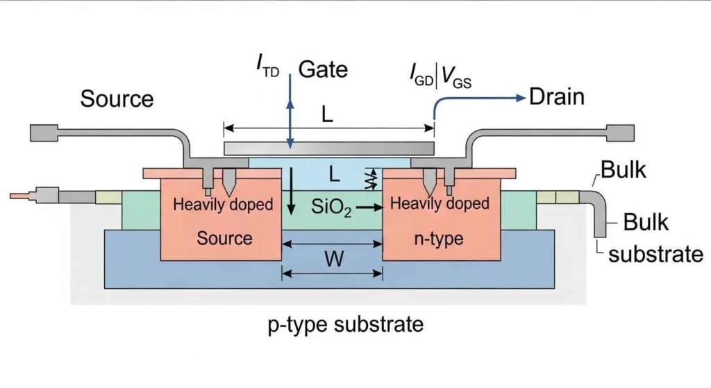
At its core, a MOSFET has three main terminals: gate, drain, and source. The gate is insulated by a thin oxide layer from the semiconductor body, creating the metal-oxide part of its name. In an N-channel MOSFET, the source and drain are N-type regions in a P-type substrate. The MOSFET diagram shows the gate controlling the channel between drain and source. Key components include the body diode, a parasitic element that can conduct in reverse, useful for protection but sometimes a limitation in switching speed. Understanding the MOSFET pin diagram is crucial: gate for control, drain for output, source for reference. The MOSFET symbol varies for N and P channels, with an arrow indicating the body diode direction.
N-Channel MOSFET as a Switch
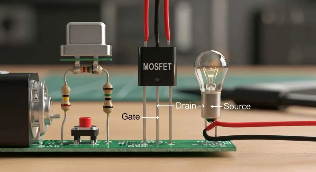
An N-channel MOSFET switch is popular for low-side switching, where it connects the load to ground. To turn it on, apply a positive voltage to the gate relative to the source, above the Vgs threshold. In a basic circuit, connect the load between the positive supply and drain, source to ground, and gate to a control signal. When the gate is high, current flows through the load. This setup is efficient for driving LEDs or small motors. For example, using an IRF540 MOSFET, a common choice for beginners, you can switch up to 33A at 100V. Ensure the gate voltage fully saturates it to minimize Rds on and heat.
P-Channel MOSFET as a Switch
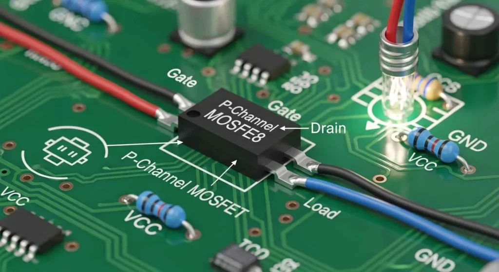
A P-channel MOSFET switch excels in high-side switching, connecting the load to the positive supply. It turns on with a negative gate voltage relative to the source. In practice, pull the gate low to activate. This is handy when you need to isolate the load from ground. A simple circuit has the source to positive supply, drain to load, and gate controlled by a pull-down signal. Models like the IRF630 work well here, handling up to 9A at 200V. Remember, P-channel MOSFETs often have higher Rds on than N-channel, so they’re better for moderate currents.
MOSFET vs BJT as a Switch
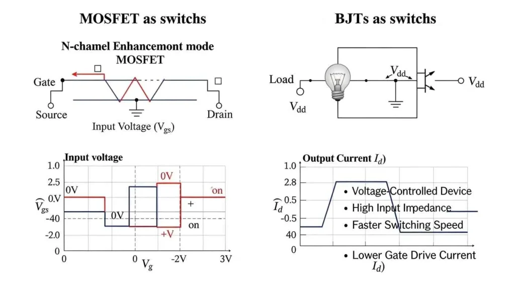
Choosing between a MOSFET and a BJT as a switch depends on your needs. BJTs are current-controlled, requiring base current to operate, which can waste power. MOSFETs are voltage-controlled, drawing almost no gate current in steady state, making them more efficient.
MOSFETs switch faster and handle higher voltages, but BJTs are cheaper for low-power tasks. In high-current applications, MOSFETs shine with lower on-resistance. However, BJTs might be simpler for beginners in some circuits.
MOSFET vs BJT as a Switch: Key Differences
While both transistor types function as switches, MOSFETs generally dominate high-power, high-frequency applications due to their speed and efficiency.
| Feature | MOSFET | BJT (Bipolar Junction Transistor) |
|---|---|---|
| Control Mechanism | Voltage-driven (Gate voltage VGS creates the channel). | Current-driven (Base current controls collector current ). |
| Switching Speed | Faster (Limited only by gate capacitance/charge). | Slower (Limited by charge storage time in the base). |
| On-State Power Loss | Lower I D 2 ⋅ R D S on. High efficiency in high current. | Higher . Typically used for low-speed/low-power. |
| Primary Applications | SMPS, Motor Drivers, Power Inverters. | Signal Amplifiers, low-speed switching. |
Basic MOSFET Switch Circuit Diagram
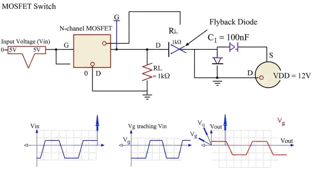
Let’s build a simple MOSFET switch circuit. Start with an N-channel like the IRF540. Connect a 12V power supply positive to a 100-ohm resistor in series with an LED, then to the drain. Source goes to ground. Gate connects to a 5V microcontroller pin through a 1k ohm resistor for protection.
When the pin goes high, the LED lights. For P-channel, reverse the logic: source to 12V, drain to LED positive, LED negative to ground via resistor, gate pulled low to turn on. This circuit demonstrates the MOSFET on off switch behavior clearly.
How to Use MOSFET as a Switch
Using a MOSFET as a switch starts with selecting the right type. Check the datasheet for Vgs threshold, Rds on, and maximum ratings. Connect probes carefully: gate for control, drain for load output, source for reference. Apply voltage above threshold to turn on. For microcontrollers, ensure logic levels match; use a MOSFET gate driver if needed for high speeds. Test with a multimeter: measure voltage drop across drain-source when onit should be near zero.
MOSFET Gate Driver and Protection
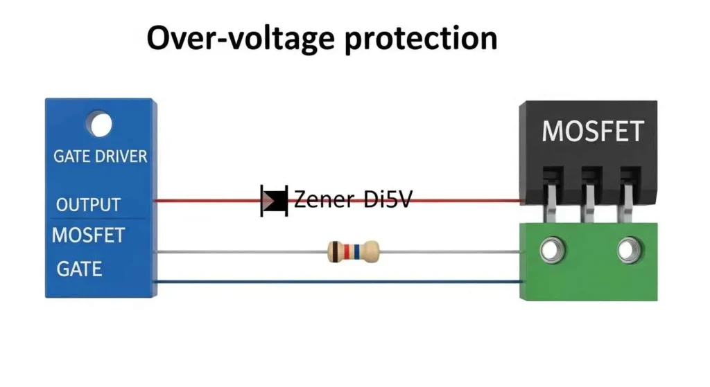
For fast switching, a MOSFET gate driver is essential. The gate acts like a capacitor, needing quick charge/discharge. Drivers provide high current pulses to speed this up. Add protection: a series resistor limits current, a Zener diode clamps voltage. For inductive loads, use a flyback diode across the load to handle back EMF. In microcontroller setups, a simple transistor driver can suffice for low frequencies.
Common Issues and Fixes: MOSFET Troubleshooting
The majority of MOSFET failures stem from thermal issues, inadequate gate drive, or circuit layout mistakes.
| Symptom / Issue | Cause | Professional Fix |
|---|---|---|
| Overheating / Failure (Thermal) | Excessive conduction loss due to high current and high . | Choose a MOSFET with lower R D S on for the operating temperature, or implement a dedicated heat sink. |
| Gate Drive Failure / Slow Switching | Gate charge Qg is too high for the drive current, or insufficient VGS voltage. | Use a dedicated Gate Driver IC to supply the necessary current. Ensure V GS is high enough to reach the lowest R D S on plateau. |
| Switching Losses are High | Slow transition times (t r , t f) due to high gate resistance (R G). | Optimize gate resistance R G Lower R G speeds up switching but increases potential gate oscillation. |
| Catastrophic Shoot-Through | Zero or insufficient dead time in an H-Bridge circuit. | Implement guaranteed Dead Time logic in the controller to ensure complementary switches are never ON simultaneously. |
Practical Applications of MOSFET as a Switch
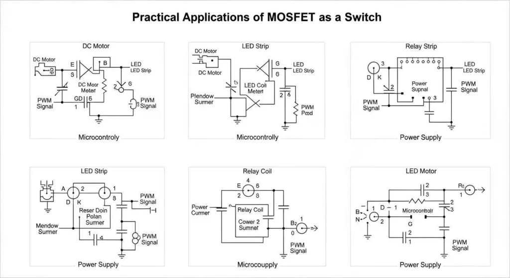
MOSFET applications abound in electronics. Use a MOSFET for LED switch in lighting: control brightness with PWM. In motor control, an H-bridge with MOSFETs allows direction reversal. For power supplies, MOSFETs switch voltages efficiently. In audio amps, they handle signal switching. Even in solar chargers, they regulate power flow. A real-world example: in a robot, use MOSFETs to switch wheel motors on command.
Quantified Case Studies: MOSFETs in Power Systems
Case 1: Switched-Mode Power Supplies (SMPS)
MOSFETs are the primary switch in all modern SMPS (Buck, Boost, etc.). In these circuits, the device must operate at very high frequencies (often >100 kHz) to keep inductors and capacitors small. This requirement directly uses the switching time formula:
- Design Challenge: Since the switching loss ( P D sw ) is dominant at high frequencies, the MOSFET must have an exceptionally low Total Gate Charge ( Q g ) and be driven by a high-current gate driver to ensure rapid transition times.
- Application: High-efficiency power conversion for laptops and server power supplies.[Image of Block diagram of Edge AI system]
Case 2: Motor Drivers (H-Bridge Circuits)
In a motor control H-Bridge, four MOSFETs control current direction. The critical design parameter is safety and preventing catastrophic failure (shoot-through):
- Design Challenge: The controller must implement a Dead Time τ dead a deliberate delay between turning one MOSFET OFF and turning its complement ON. This prevents both transistors on a leg from short-circuiting the supply.
- Professional Requirement: τ dead must always be greater than the maximum t off time of the slower MOSFET.
Case 3: Microcontroller GPIO Interfacing
A microcontroller’s GPIO pin (often 3.3V or 5V) cannot directly supply the current to run a 12V fan or LED strip. A MOSFET acts as the intermediary switch:
- Design Requirement: A Logic-Level MOSFET must be selected, meaning its threshold voltage V GS this low enough (typically <2V) to be fully saturated by the 3.3V or 5V GPIO pin, guaranteeing minimal R D S on and low power loss.
MOSFET for Motor Control
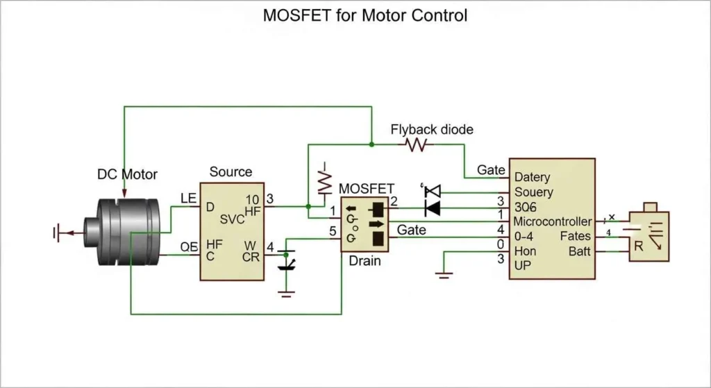
Controlling motors with MOSFETs is straightforward. For DC motors, a single N-channel MOSFET switches power. Add PWM for speed control. An H-bridge uses four MOSFETs for bidirectional control. Ensure dead time to avoid shoot-through current. Models like IRF540 handle motor currents well, but calculate heat dissipation: power loss equals current squared times Rds on.
MOSFET Heat Dissipation and Protection
Heat is a MOSFET’s enemy. During switching, losses occur in transitions. Minimize with fast drivers. Calculate heat: use Rds on and current to find power dissipation, then select a heatsink if over 1W. Protection includes overvoltage clamps, current limiting, and thermal shutdown circuits.
Advantages and Disadvantages of MOSFET as a Switch
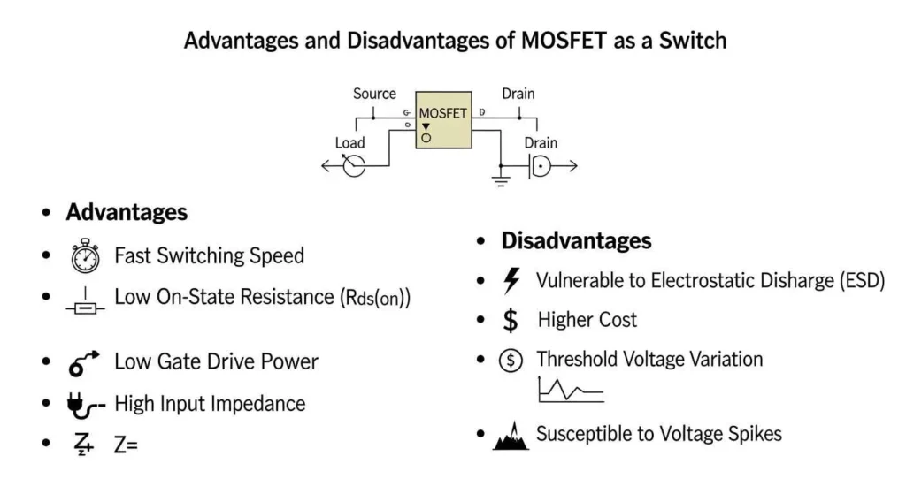
MOSFET advantages include fast switching, low power loss, and high efficiency. They’re compact and reliable. Disadvantages: sensitive to static, higher cost than BJTs, and need careful gate driving. Overall, for modern designs, advantages outweigh drawbacks.
Simple Experiments for Beginners
Try this: Build a MOSFET LED blinker. Use an Arduino to pulse the gate. Observe how gate voltage affects brightness. Another: Switch a small fan. Measure current and voltage drop to see efficiency. These hands-on tests build intuition.
Industry Standards: Selection and Thermal Reliability
Selecting and operating a MOSFET reliably requires strict adherence to datasheet parameters and industry-defined thermal standards.
JEDEC and Datasheet Parameters
- JEDEC Standards: The Joint Electron Device Engineering Council (JEDEC) defines testing procedures and maximum ratings for power semiconductors. Always apply a 20% derating margin to the maximum voltage and current ratings specified in the datasheet for safety.
- R D S on: On-state resistance. This value is critical as it directly determines conduction loss. Note that R D S on increases with temperature, making thermal management crucial.
- V GS th </: Gate-Source Threshold Voltage. Defines the voltage at which the MOSFET begins to turn on. The maximum value must be considered when designing logic interfaces.
- Q g (Total Gate Charge): The charge required to switch the device. This is the primary metric for calculating the necessary gate drive current and speed.
Thermal Resistance and IEC Safety
Reliability hinges on keeping the internal junction temperature ( T J ) below its maximum rating (typically 150 ° C to 175 ° C).
- Thermal Resistance θ JC: The datasheet provides the thermal resistance from the Junction to the Case. This value is essential for calculating the required size of an external heatsink.
- IEC Safety Ratings: For power electronics, compliance with IEC safety standards ensures that insulation (creepage and clearance distances) and component spacing are adequate to prevent shock and fire hazards.
Conclusion
Mastering the MOSFET as a switch unlocks endless possibilities in electronics. From basic circuits to advanced controls, its efficiency and speed make it indispensable. Experiment with the ideas here, and you’ll see why it’s a favorite. Share your MOSFET projects in the comments or download our free circuit guide!
Frequently Asked Questions (FAQ)
What is the formula for MOSFET drain current?
In the saturation region (which defines the maximum current capacity), the drain current ( I D ) is approximated by the square-law relationship: I D ≈ k ⋅ V GS – V TH 2 . This shows that the current capacity increases quadratically as the gate-source voltage ( V GS ) increases above the threshold voltage ( V TH ).
Why are MOSFETs preferred over BJTs in switching applications?
MOSFETs are voltage-driven, meaning they require almost zero continuous current to stay ON, leading to much higher energy efficiency. They also have much faster switching speeds (lower t r , t f ) and lower on-state resistance ( R D S on ), making them superior for high-frequency applications like SMPS and high-current motor drivers.
How do you troubleshoot overheating in MOSFETs?
The first step is to check if the power loss is dominated by conduction loss ( I D 2 ⋅ R D S on ) or P D sw , switching loss. If it is conduction loss, choose a MOSFET with a lower R D S on or ensure the existing one has a properly sized heat sink. If it is switching loss (common at high frequency), use a dedicated gate driver IC to reduce the transition times.
What is the importance of Total Gate Charge (Q_g)?
Total Gate Charge is the amount of electrical charge needed to fully turn the MOSFET ON. It is the key parameter for selecting a gate driver, as the driver must be capable of delivering enough peak current to charge the gate capacitance quickly, thereby minimizing switching time and loss.
What is the role of RDS(on) in MOSFET efficiency?
Lower RDS(on) reduces conduction losses (ID2⋅RDS(on)), improving efficiency in high‑current applications.
How does switching frequency affect MOSFET power loss?
Higher frequency increases switching losses (PDsw), requiring faster gate drivers and careful thermal design.
What is the safe operating area (SOA) of a MOSFET?
SOA defines the limits of voltage, current, and time where the MOSFET can operate safely without damage.
Why is gate resistance (Rg) important in MOSFET design?
Gate resistance controls the charging/discharging speed of the gate, balancing switching speed and EMI.
How do you calculate MOSFET switching losses?
Switching losses are approximated as PDsw=12⋅VDS⋅ID⋅(tr+tf)⋅fsw.
What is the significance of threshold voltage (VTH)?
VTH determines the minimum gate‑source voltage required to turn the MOSFET ON; lower VTH enables logic‑level control.
How does body diode behavior affect MOSFET performance?
The intrinsic body diode can cause reverse recovery losses in switching applications, impacting efficiency in synchronous rectifiers.
What design standards ensure reliable MOSFET operation?
Standards include proper derating (operating below max ratings), thermal management, EMI compliance, and adherence to IEC/JEDEC reliability guidelines.
Having read this I thought it was very informative. I appreciate you taking the time and effort to put this article together. I once again find myself spending way to much time both reading and commenting. But so what, it was still worth it!