How a Transistor Works: Construction, Physics, Biasing, Gain & Applications
The Guide from semiconductor physics and P-N junctions to NPN/PNP biasing, current gain (β), switching, amplification, MOSFETs, and real-world circuit design.
🎯 Key Takeaways
- ✅ A transistor is a three-terminal semiconductor device that uses a small input signal to control a much larger output current enabling amplification and switching
- ✅ BJT transistors are current-controlled: base current (IB) controls collector current (IC) with a gain of β = IC/IB, typically 100–500
- ✅ The three operating regions are cutoff (OFF), active (amplifier), and saturation (ON) understanding which region you're in is fundamental to all transistor circuit design
- ✅ For a silicon BJT to conduct, the base-emitter junction must be forward biased to ≈ 0.6–0.7V
- ✅ MOSFETs are voltage-controlled and dominate digital logic, power electronics, and modern ICs a single chip contains billions of MOSFETs
- ✅ Proper voltage divider biasing is the most reliable method to set a stable Q-point in the active region for linear amplification
- ✅ Transistors are the fundamental building block of all modern electronics from the 2N2222 in a hobbyist circuit to 3nm FinFETs in a modern CPU
What Every Engineer Must Know About Transistors
For silicon, the base-emitter junction always drops ≈0.7V when conducting. This is the P-N junction forward voltage bake it into every circuit calculation from day one.
The same transistor part number can have β ranging from 100 to 500. Always design circuits to work across the full β range. Voltage divider bias does this automatically.
VBE decreases ≈2mV/°C as temperature rises. This increases collector current with heat, which further raises temperature thermal runaway is a real failure mode in power BJTs.
Unlike BJTs, MOSFETs have virtually infinite input impedance. Gate current is effectively zero in DC conditions making them ideal for microcontroller GPIO outputs driving power loads.
A saturated BJT drops only 0.2V from collector to emitter. When switching, always drive base current hard enough (IB ≥ IC/β_min) to ensure full saturation and minimal switch losses.
Every digital logic gate in a CPU is a CMOS pair one NMOS and one PMOS. When one is ON the other is OFF, so static current is near-zero. This is why CMOS dominates digital design.
How Does a Transistor Work? (60-Second Answer)
A transistor is a three-terminal semiconductor device Base, Collector, and Emitter in a BJT that allows a small signal at the base to control a much larger current flowing from collector to emitter. It is made from two back-to-back P-N junctions formed by doping a semiconductor (usually silicon) with impurities to create regions with excess electrons (N-type) or excess holes (P-type).
When the base-emitter junction is forward biased (VBE ≈ 0.7V for silicon), electrons injected from the emitter cross the thin base layer and are swept into the collector by the reverse-biased collector-base junction. The collector current IC is β times the base current IB. This current amplification is the core transistor action and by operating in different regions (cutoff, active, saturation), the same device can function as both a switch and a linear amplifier.
📋 Table of Contents
- Semiconductor Physics: N-Type, P-Type & the P-N Junction
- BJT Construction: Emitter, Base & Collector Regions
- Working Principle: How Transistor Action Occurs
- Three Operating Regions: Cutoff, Active & Saturation
- Core Formulas: Gain, Biasing & Operating Point
- NPN vs PNP: Construction, Biasing & Usage
- Transistor Biasing: Voltage Divider & Q-Point Stability
- Transistor as a Switch: Cutoff to Saturation
- Transistor as an Amplifier: Common-Emitter Configuration
- MOSFETs: Enhancement & Depletion Mode Operation
- BJT vs MOSFET: Engineering Comparison
- Case Studies: LED Driver, Audio Amp & H-Bridge
- Real-World Applications Across Industries
- Advantages & Limitations
- The Transistor's Origin: Bell Labs 1947 & Evolution Timeline
- Real Component Comparison: 2N2222 vs BC547 vs IRFZ44N
- Common Mistakes Engineers Make (with Fixes)
- Transistor Troubleshooting Guide: Field Diagnostics
- FAQ: 12 Common Engineering Questions
Semiconductor Physics: N-Type, P-Type & the P-N Junction
To understand how a transistor works, you must first understand what a semiconductor is and what happens at a P-N junction. Silicon, the most common transistor material, is a semiconductor it conducts electricity only under certain conditions, unlike a conductor (copper) or insulator (rubber).
Pure silicon has four valence electrons and forms a regular crystal lattice with no free carriers. To make it useful, we dope it we add controlled amounts of specific impurities:
- N-type silicon: Doped with a Group V element (phosphorus, arsenic). Each dopant atom has 5 valence electrons 4 bond with silicon, leaving one free electron. N-type silicon has an excess of electrons (negative charge carriers). Majority carriers are electrons.
- P-type silicon: Doped with a Group III element (boron, aluminum). Each dopant atom has only 3 valence electrons when bonded into the silicon lattice, it leaves a "hole" (a missing electron that behaves as a positive charge carrier). Majority carriers are holes.
What Is the P-N Junction?
When P-type and N-type silicon are joined, a P-N junction forms at the boundary. Electrons from the N-side diffuse toward the P-side and recombine with holes. This creates a region depleted of free carriers the depletion region with a built-in electric field pointing from N to P.
This built-in field eventually stops further diffusion, establishing equilibrium. The P-N junction is the fundamental building block of all semiconductor devices: diodes, transistors, solar cells, and LEDs.
Forward biasing (positive voltage on P, negative on N) narrows the depletion region and allows current to flow the junction conducts once VF ≈ 0.7V for silicon. Reverse biasing (positive on N, negative on P) widens the depletion region virtually no current flows. This directional behavior is the foundation of transistor operation.
BJT Construction: Emitter, Base & Collector Regions
A Bipolar Junction Transistor (BJT) consists of three layers of doped semiconductor with two P-N junctions. In an NPN transistor, the structure is N-P-N: a heavily doped N-type emitter, a very thin and lightly doped P-type base, and a moderately doped N-type collector.
Why Each Region Is Designed As It Is
- Emitter: Heavily doped to provide a large reservoir of majority carriers (electrons in NPN). Its job is to emit carriers into the base.
- Base: Intentionally very thin (micrometers) and lightly doped. This is the control terminal. Its thinness ensures most injected carriers diffuse to the collector rather than recombining in the base this is what makes the transistor amplify.
- Collector: Moderately doped and physically larger than the emitter, designed to collect the carrier stream from the base. Its larger size handles the power dissipation from carrying the main circuit current.
Engineer's Note: Why Emitter ≠ Collector (Even Though Both Are N-type)
Students often ask: can you swap emitter and collector? Technically a BJT will still work in reverse, but the gain (β) will be 10–50× lower because the doping levels and geometry are optimized for one direction. Always connect transistors in the correct polarity.
Working Principle: How Transistor Action Occurs
The working principle of a BJT transistor can be broken down into four physical steps that occur simultaneously inside the device:
Forward Biasing the Base-Emitter Junction (J1)
A voltage VBE ≈ 0.7V is applied between base and emitter, forward biasing junction J1. This narrows the depletion region at J1 and creates a potential barrier low enough for electrons from the emitter to flow into the base region. Base current IB begins to flow.
Minority Carrier Injection Into the Base
Electrons from the N-type emitter are injected into the P-type base as minority carriers. Inside the base, these electrons are surrounded by holes (the majority carriers of P-type material). Here is the critical design point: the base is extremely thin (1–10 μm) and lightly doped, so very few electrons have time to recombine with holes before reaching the collector junction.
The Collector-Base Junction (J2) Sweeps Carriers Across
The collector-base junction is reverse biased (VCB is negative in NPN). This creates a strong electric field at J2 pointing from collector into base. When the electrons that diffused through the base reach this junction, the field sweeps them across into the collector they become collector current IC. Approximately 95–99% of injected electrons reach the collector this way.
Current Amplification: IC = β × IB
The small base current IB (representing the electrons that did recombine in the base) controls the large collector current IC. The ratio IC/IB is the transistor's DC current gain β (or hFE). Because base recombination is small by design (~1–5% of injected electrons), β is large typically 100 to 500. This is transistor action: a tiny base current controlling a large collector current.
Think of the transistor as a current-controlled tap (valve). The base current is the handle it takes very little force (current) to open it. The collector-emitter path is the pipe when the handle turns, a large flow (current) results. The ratio of "flow" to "handle force" is β. This is why transistors amplify.
Three Operating Regions: Cutoff, Active & Saturation
Every transistor circuit places the device in one of three operating regions. Understanding which region you are designing for determines everything about the circuit's behavior.
| Region | J1 (B-E) | J2 (C-B) | IC | VCE | Use Case |
|---|---|---|---|---|---|
| Cutoff OFF | Reverse biased | Reverse biased | ≈ 0 (ICEO only) | = VCC (full supply) | Transistor switch OFF state |
| Active (Linear) Amplifying | Forward biased | Reverse biased | β × IB | 0.2V – VCC | Amplifiers, linear circuits |
| Saturation Fully ON | Forward biased | Forward biased | ≈ VCC/RC (max) | ≈ 0.2V (VCE(sat)) | Transistor switch ON state |
| Breakdown Destructive | Any | Avalanche breakdown | Very large | > BVCEO | Avoid device damage |
Designing an amplifier? The transistor must stay in the active region throughout the signal swing if it clips into saturation or cutoff, the signal is distorted. Designing a switch? You want fast, clean transitions from cutoff to saturation with no time spent in the active region (which dissipates power as heat).
Core Formulas: Gain, Biasing & Operating Point
Also: IC = β × IB | IE = IC + IB = (β + 1) × IB
VE = VB − VBE ≈ VB − 0.7V | IE = VE / RE | IC ≈ IE (since β >> 1)
For active region: VCE > VCE(sat) ≈ 0.2V | For saturation: VCE ≈ 0.2V
re = 26mV / IC (intrinsic emitter resistance) | Example: IC=1mA → re=26Ω, RC=4.7kΩ → AV = −181
VGS = gate-source voltage | VTH = threshold voltage (typ. 2–4V) | Valid when VDS > VGS − VTH
Given: VCC = 12V, β = 200, IC(Q) = 1mA desired, VCE(Q) = 6V. Select RE = 1kΩ (gives IE ≈ IC = 1mA, VE = 1V). Then VB = VE + 0.7 = 1.7V. RC = (VCC − VCE − VE)/IC = (12−6−1)/1mA = 5kΩ. For voltage divider: choose bleeder current = IC/10 = 0.1mA. R2 = VB/0.1mA = 1.7V/0.1mA = 17kΩ. R1 = (VCC−VB)/0.1mA = 10.3V/0.1mA = 103kΩ (use 100kΩ standard). Check: VB = 12×17k/(17k+100k) ≈ 1.74V ✓
NPN vs PNP: Construction, Biasing & Usage
| Property | NPN Transistor | PNP Transistor |
|---|---|---|
| Structure | N-P-N (emitter N, base P, collector N) | P-N-P (emitter P, base N, collector P) |
| Majority carriers | Electrons | Holes |
| Turn-ON condition | VBE ≈ +0.7V (base more positive than emitter) | VEB ≈ +0.7V (emitter more positive than base) |
| Collector current direction | Into collector (conventional) | Out of collector (conventional) |
| Switch configuration | Low-side switch (between load and GND) | High-side switch (between VCC and load) |
| Speed / gain | Higher (electrons faster than holes) | Slightly lower |
| Common examples | 2N2222, BC547, 2N3904, TIP31 | 2N2907, BC557, 2N3906, TIP32 |
| Usage prevalence | Most Common | Complementary circuits, high-side drivers |
In 15 years of circuit design, I can count on one hand the times I chose PNP over NPN as a primary switch. PNP transistors shine in high-side switching (load between transistor and ground) and in push-pull complementary pairs (e.g., class AB audio amplifiers with NPN lower and PNP upper transistors). For any low-side switch motor driver, relay, LED driver NPN is always simpler and more intuitive.
Transistor Biasing: Voltage Divider & Q-Point Stability
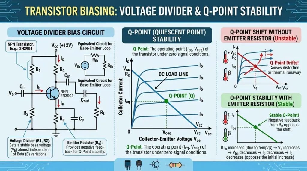
Biasing means establishing a stable DC operating point the Q-point (quiescent point) in the active region before any AC signal is applied. Without correct biasing, even a perfect transistor will not amplify linearly.
The Four Main Biasing Methods
| Bias Method | Circuit Complexity | Stability vs β Variation | Use Case |
|---|---|---|---|
| Fixed Base Bias | Simplest (1 resistor) | Poor Q-point shifts with β | Switching circuits only; never for linear amplifiers |
| Collector-to-Base Bias | Simple (1 feedback resistor) | Moderate self-correcting but incomplete | Simple amplifiers with moderate stability requirements |
| Emitter-Stabilized Bias | Moderate (adds RE) | Good RE provides negative feedback | Audio stages, general amplifiers |
| Voltage Divider Bias Recommended | Standard (R1, R2, RC, RE) | Excellent nearly β-independent when R1∥R2 << β×RE | All professional amplifier and linear circuit design |
Why Voltage Divider Bias Is Always Preferred
The voltage divider (R1, R2) sets VB independently of transistor β provided the current through the divider is much larger than IB (typically 10× larger). Since VB is fixed by R1/R2 and VBE is fixed at 0.7V, the emitter voltage VE = VB − 0.7V is also fixed. Therefore IC ≈ IE = VE/RE is determined by external resistors, not by β. Even if you replace one transistor with another of the same type but different β, the Q-point barely moves. This is the hallmark of a well-designed circuit.
Professional Design Rule: Q-Point at VCC/2
For maximum undistorted output swing in a common-emitter amplifier, set VCE(Q) ≈ VCC/2. This centers the output on the load line, giving equal headroom for positive and negative signal swings. The remaining VCC/2 is divided between VRC and VRE. A common split: VCE = VCC/2, VRC = VCC/3, VRE = VCC/6.
Transistor as a Switch: Cutoff to Saturation
When used as a switch, the transistor operates only in cutoff (OFF) or saturation (ON) spending as little time as possible in the active region (which dissipates power). This is the mode used in digital logic, relay drivers, LED drivers, motor control, and power electronics.
Designing the Switch: Ensuring Full Saturation
For reliable switching, you must guarantee IB is large enough to saturate the transistor across the full range of β variation. The rule is:
RB = (VIN − VBE) / IB | VBE = 0.7V | Typical RB for microcontroller GPIO: 1kΩ – 10kΩ
Design a transistor circuit to drive a 12V relay coil (80mA) from Arduino's 5V GPIO (20mA max output)
Given: Relay coil current IC = 80mA, VCC(relay) = 12V, GPIO = 5V, transistor: 2N2222 (β_min = 100)
Step 1: Minimum base current = IC/β_min = 80mA/100 = 0.8mA. Use 5× safety margin → IB = 4mA (well within 20mA GPIO limit)
Step 2: RB = (VGPIO − VBE) / IB = (5 − 0.7) / 4mA = 4.3V / 4mA = 1.075kΩ → use 1kΩ standard
Step 3: Add a flyback diode (1N4007) across the relay coil relay coils are inductive and generate a large reverse voltage spike when switched OFF that will destroy the transistor without protection.
Step 4: Check power dissipation in saturation: P = VCE(sat) × IC = 0.2V × 80mA = 16mW well within 2N2222's 625mW rating ✓
Relays, solenoids, motors, and any inductive load will generate a voltage spike (V = L × dI/dt) when the transistor turns OFF and current collapses. This spike can be 10–100× VCC. A single 1N4007 reverse-biased across the inductive load clamps this spike and protects the transistor omitting it is the most common cause of transistor failure in switching circuits.
The common-emitter (CE) configuration is the most widely used transistor amplifier topology. It provides voltage gain, current gain, and power gain simultaneously with a 180° phase inversion between input and output.
Common-Emitter Amplifier: Key Parameters
| Parameter | Common Emitter | Common Base | Common Collector (Emitter Follower) |
|---|---|---|---|
| Voltage Gain (AV) | High (100–1000+) Best | High (similar to CE) | <1 (≈1) voltage buffer |
| Current Gain (AI) | High (≈β) | <1 | Highest (≈β+1) |
| Input Impedance | Medium (1kΩ – 5kΩ) | Very Low | Very High (β×RE) |
| Output Impedance | High (≈RC) | Very High | Very Low (≈RE∥(re+RS/β)) |
| Phase Shift | 180° (inverting) | 0° (non-inverting) | 0° (non-inverting) |
| Primary Use | Voltage amplification | RF/high-frequency | Impedance matching, buffer |
Design Insight: Why Use Emitter Bypass Capacitor?
In a CE amplifier, adding RE improves DC bias stability but reduces AC voltage gain because the AC signal also sees RE in the gain formula: AV = −RC/(re + RE). A bypass capacitor CE in parallel with RE short-circuits RE at AC frequencies, restoring gain to AV = −RC/re, while the DC bias stability from RE is maintained. This is one of the most important tricks in analog amplifier design.
We designed a microphone preamplifier for an industrial noise monitoring system. A standard CE stage with 2N3904, VCC = 9V, IC(Q) = 1mA gave AV ≈ 180 (45 dB). Adding a bypass capacitor on RE reduced noise referral from the bias network by 12 dB and extended usable bandwidth from 800Hz to 18kHz turning a mediocre prototype into a production-ready circuit in one component change.
MOSFETs: Enhancement & Depletion Mode Operation
The MOSFET (Metal-Oxide-Semiconductor Field-Effect Transistor) is the dominant transistor type in modern electronics. Unlike the BJT, which is current-controlled, the MOSFET is voltage-controlled its gate draws virtually no DC current, making it easy to drive from microcontrollers and logic circuits.
How the MOSFET Channel Forms
In an N-channel enhancement MOSFET, the gate is separated from the semiconductor by an ultra-thin layer of silicon dioxide (SiO₂) a near-perfect insulator. When VGS is applied:
- The positive gate voltage repels holes from the P-type substrate surface beneath the gate
- Electrons are attracted to this surface, accumulating until an inversion layer forms
- This inversion layer is an induced N-type channel connecting source to drain
- Once VGS exceeds the threshold voltage VTH (typically 2–4V), the channel is strong enough to conduct drain current ID
| MOSFET Type | Channel | Normally ON/OFF at VGS=0 | Turn ON Condition | Common Use |
|---|---|---|---|---|
| N-ch Enhancement Most Common | N-type (induced) | OFF | VGS > VTH (+2 to +4V) | Digital logic, power switching, motor drivers |
| P-ch Enhancement | P-type (induced) | OFF | VGS < −VTH (negative) | High-side switches, CMOS logic (PMOS half) |
| N-ch Depletion | N-type (built-in) | ON | VGS < 0 to pinch off | Constant current sources, RF JFETs |
| P-ch Depletion | P-type (built-in) | ON | VGS > 0 to pinch off | Rare; specialized analog circuits |
MOSFETs win in digital design because their near-infinite input impedance means they draw no static gate current only dynamic current to charge/discharge gate capacitance. This allows billions of CMOS gates to switch at GHz frequencies within a practical power budget. CMOS (Complementary MOS = NMOS + PMOS pairs) is the reason modern CPUs exist.
BJT vs MOSFET: Engineering Comparison
| Property | BJT | MOSFET |
|---|---|---|
| Control type | Current-controlled (IB controls IC) | Voltage-controlled (VGS controls ID) |
| Input impedance | Medium (1kΩ–50kΩ typical) | Extremely high (GΩ gate is insulated) |
| Drive requirement | Base current (continuous during ON) | Gate voltage only (capacitive no DC current) |
| ON-state loss | VCE(sat) × IC (0.2V × IC) | ID² × RDS(on) can be milliohms in power MOSFETs |
| Switching speed | Slower (minority carrier storage in base) | Faster (majority carrier device) |
| Thermal stability | Poor VBE decreases with T → thermal runaway risk | Good RDS(on) increases with T (self-limiting) |
| Noise in analog | Lower noise in small-signal RF/audio | Higher flicker (1/f) noise less ideal for audio |
| High voltage | Good (up to 1000V Darlington types) | Excellent SiC MOSFETs rated 1200V+ |
| High current | Good (power BJTs to 50A) | Excellent (paralleling easy due to positive TC) |
| Cost (discrete) | Cheaper at low volumes | Comparable; significantly cheaper in ICs |
| Best for | Audio amplifiers, RF, low-cost switching | Digital logic, power electronics, battery devices |
✅ Choose a BJT When:
- Designing audio or RF amplifiers requiring low noise
- Cost is critical and switching speed is <100kHz
- You need well-understood, predictable VBE behavior
- Designing a current mirror or differential pair (BJT excels here)
- Working with legacy circuit designs
✅ Choose a MOSFET When:
- Driving from a microcontroller GPIO with no drive circuit
- Power switching at >100kHz (PWM motor drives, SMPS)
- Battery-powered devices (near-zero gate drive power)
- Designing digital logic or any IC-level circuit
- Paralleling devices for high current (positive TC prevents hogging)
Case Studies: LED Driver, Audio Amp & H-Bridge Motor Control
Problem: Drive 24 high-brightness LEDs (20mA each) from a 3.3V microcontroller GPIO
Challenge: GPIO cannot supply 480mA total. Individual GPIO output: 8mA max. Need to multiply current by ~60×.
Solution: BC817 NPN transistor (β_min = 100, 500mA collector rating) per LED bank of 12. GPIO → RB(4.7kΩ) → Base. IC = 240mA per transistor (12 LEDs × 20mA). Required IB = 240mA/100 = 2.4mA → with RB = 4.7kΩ: IB = (3.3−0.7)/4.7k = 0.55mA. Too low revise to RB = 1kΩ → IB = 2.6mA ✓, transistor saturates at forced β = 240mA/2.6mA = 92 (< β_min = 100) ✓
Result: Each GPIO pin drives 12 LEDs reliably. Total board LED current = 480mA, entirely handled by transistors. GPIO sees only 3.3mA per channel.
Problem: Bidirectional control of a 24V DC brushed motor (5A) from a 3.3V PWM signal
Challenge: Need to reverse motor direction and vary speed. Voltage levels don't match. High switching frequency (20kHz PWM) requires fast switching device.
Solution: H-bridge using two N-channel MOSFETs (IRF540N: RDS(on) = 44mΩ, VGS(th) = 4V) and two P-channel MOSFETs (IRF9540N) with a gate driver IC (IR2104) to boost 3.3V logic to 12V gate drive. At 5A and 44mΩ: conduction loss per MOSFET = 5² × 0.044 = 1.1W. Full H-bridge = 2.2W at any time. Switch losses at 20kHz calculated separately.
Result: Full bidirectional motor control, 0–100% speed via PWM, total efficiency > 94% at full load. BJT alternative would dissipate 3–5× more power in the on-state (VCE(sat) vs RDS(on)).
Failure Analysis: Audio amplifier output stage fails after 30 minutes of operation
Symptoms: TIP41C NPN transistors in class AB output stage worked fine at room temperature. After 30 minutes playing at half power, transistors went into thermal runaway and destroyed themselves.
Root Cause: Fixed base bias without thermal feedback. As temperature rose, VBE decreased (~2mV/°C), increasing IB, increasing IC, increasing dissipation, further raising temperature a positive feedback loop. No emitter resistor to provide negative feedback. No thermistor on bias circuit.
Fix: Added 0.47Ω emitter resistors (degeneration) to each output transistor, plus a VBE multiplier circuit with a transistor mounted on the heatsink as a thermal sensor. Result: stable thermal operating point across 20°C–80°C ambient range. No failures in 3-year production run.
Real-World Applications Across Industries
| Application | Transistor Type | Function | Industry |
|---|---|---|---|
| Smartphone CPU | N-ch MOSFET (3nm FinFET) | Digital logic switching at GHz | Consumer electronics |
| Audio power amplifier | Complementary BJT pair | Class AB linear amplification | Audio / consumer |
| Solar inverter | SiC MOSFET / IGBT | DC-AC power conversion at 1200V | Renewable energy |
| Electric vehicle motor drive | SiC MOSFET (1200V) | 3-phase PWM inverter | Automotive / EV |
| RF transmitter (4G/5G base station) | GaN HEMT | High-power RF amplification | Telecommunications |
| Switching power supply (SMPS) | N-ch MOSFET | High-frequency DC-DC conversion | Power electronics |
| Hearing aid | BJT / small-signal MOSFET | Low-noise audio amplification | Medical devices |
| Industrial PLC output module | NPN BJT / MOSFET | Relay driving, solenoid control | Industrial automation |
| LED streetlight driver | N-ch MOSFET | Constant current PWM control | Lighting |
| Medical imaging (MRI gradient amp) | IGBT module | Precise high-current switching | Medical |
| Satellite transponder | GaAs MESFET/HEMT | Low-noise microwave amplification | Aerospace |
| DRAM memory cell | N-ch MOSFET | Charge storage access switch | Semiconductor |
Advantages & Limitations of Transistors
✅ Advantages
- Extremely small, lightweight, and low-power vs vacuum tubes
- Highly reliable no moving parts, no thermionic emission degradation
- Can be fabricated billions per chip at nanometer scale
- Operates at GHz switching speeds (MOSFETs)
- Wide voltage (0V – 1200V+) and current range (μA – kA)
- Low cost commodity BJTs cost <$0.01 in volume
- Bidirectional in some configurations (AC switches)
- Can be integrated alongside other components on a single die
⚠️ Limitations
- BJTs susceptible to thermal runaway without proper thermal design
- MOSFET gates sensitive to electrostatic discharge (ESD)
- β varies widely between units of same part number
- High-power transistors require heatsinking
- MOSFET body diode can cause issues in some topologies
- Minority carrier storage in BJT limits switching speed
- Require careful PCB layout at high frequencies
Future Trends: FinFETs, GaN, SiC & 2D Transistors
The transistor has evolved dramatically from the first point-contact germanium device at Bell Labs in 1947. The modern landscape reveals several critical frontiers:
FinFET & Gate-All-Around (GAA) Transistors
Planar MOSFETs hit fundamental limits below 22nm quantum tunneling allows current to flow even when the gate is "off." Intel's FinFET (fin-shaped 3D channel) solved this from 22nm onwards. At 3nm and below, Samsung and TSMC have transitioned to Gate-All-Around (GAA) or Nanosheet transistors where the gate wraps around a silicon nanosheet on all four sides for better channel control. Apple's A17 Pro and M3 chips use 3nm processes with billions of GAA-style transistors.
Wide Bandgap Semiconductors: GaN and SiC
Silicon has fundamental limits in power and frequency applications. Gallium Nitride (GaN) and Silicon Carbide (SiC) have larger bandgaps (3.4 eV and 3.3 eV vs silicon's 1.1 eV), enabling:
- GaN HEMTs: Operate at frequencies up to 100GHz with high breakdown voltage used in 5G base stations, radar, and satellite systems. GaN power devices (EPC, GaN Systems) enable switching at 1–10MHz for ultra-compact power supplies
- SiC MOSFETs: Rated to 1700V with RDS(on) an order of magnitude lower than silicon at the same voltage now standard in EV motor drives (Tesla, BYD), industrial inverters, and solar systems
2D Material Transistors
Beyond silicon, 2D materials like graphene (zero bandgap currently not ideal for switching) and molybdenum disulfide (MoS₂, bandgap ≈ 1.8 eV) are being investigated for transistors at the 1nm node and below. IBM demonstrated a MoS₂ transistor with a gate length of 1nm in 2016. These remain research-stage but represent the potential successor to silicon CMOS beyond the 2030s.
The most immediately impactful trend for power electronics engineers is the mainstream adoption of SiC MOSFETs in EV inverters and GaN transistors in consumer power adapters. Prices have dropped 5–10× since 2018. If you design any power conversion circuit today and aren't at least evaluating GaN/SiC, you are designing with yesterday's components.
The Transistor's Origin: Bell Labs, 1947 Why It Changed Everything
William Shockley, John Bardeen, and Walter Brattain at Bell Telephone Laboratories demonstrated the first working point-contact transistor. It was made from germanium, operated at room temperature, and amplified audio signals replacing fragile, power-hungry vacuum tubes. All three inventors received the Nobel Prize in Physics in 1956. The device they built weighed a few grams; today, a single Apple M-series chip contains more transistors than there are stars in the Milky Way galaxy.
From Germanium to Silicon to Silicon Carbide: 78 Years of Evolution
| Era | Key Device | Material | Gate Length / Size | Milestone |
|---|---|---|---|---|
| 1947 | Point-contact transistor | Germanium | ~1 cm | First working transistor Bell Labs (Bardeen, Brattain, Shockley) |
| 1954 | Junction transistor (BJT) | Silicon | ~mm scale | First silicon transistor Texas Instruments (Gordon Teal) |
| 1960 | MOSFET | Silicon | ~20 µm | Kahng & Atalla at Bell Labs foundation of all digital ICs |
| 1971 | Intel 4004 CPU | Silicon | 10 µm | First commercial microprocessor 2,300 transistors |
| 2006 | Intel Core 2 Duo | Silicon | 65 nm | 291 million transistors personal computing mainstream |
| 2020 | Apple M1 | Silicon (5nm) | 5 nm | 16 billion transistors laptop/desktop performance redefined |
| 2023 | Apple M3 Ultra | Silicon (3nm) | 3 nm | 184 billion transistors GAA nanosheet architecture |
| 2024+ | SiC MOSFET / GaN HEMT | SiC / GaN | varies | Wide bandgap EV inverters, 5G base stations, space systems |
Every time I pick up a BC547 to debug a student circuit, I think about Bardeen and Brattain hunched over their germanium chip in 1947. That device and this cheap 10-cent transistor operate on the exact same physics minority carrier injection, depletion region modulation, current amplification. The package changed. The physics did not. Understanding the physics means you understand every transistor ever made, and every transistor that will ever be made.
Real Transistor Comparison: 2N2222 vs BC547 vs IRFZ44N Actual Parameters
Generic tutorials talk about "a transistor" in abstract. Real engineers select specific parts. Here is a definitive comparison of the three most commonly used transistors in hobbyist and industrial electronics with actual datasheet values, not estimates.
| Parameter | 2N2222 (NPN BJT) | BC547 (NPN BJT) | IRFZ44N (N-ch MOSFET) |
|---|---|---|---|
| Type | NPN BJT General Purpose | NPN BJT Low-Power Signal | N-Channel Enhancement MOSFET |
| Manufacturer | Multiple (ON Semi, Fairchild, ST) | Multiple (Vishay, Philips, Mouser) | Vishay / International Rectifier |
| Datasheet | onsemi.com P2N2222A | vishay.com BC546-547 | vishay.com IRFZ44N |
| Max collector/drain current (IC/ID) | 600 mA | 100 mA | 49 A |
| Max voltage (VCEO / VDS) | 40 V | 45 V | 55 V |
| DC Current Gain (hFE / β) | 100–300 (typ. 150 at IC=10mA) | 110–800 (typ. 200 at IC=2mA) | N/A (voltage-controlled) |
| VBE / VGS(th) | 0.6–0.7 V | 0.58–0.7 V | 2–4 V (threshold) |
| VCE(sat) / RDS(on) | 0.3 V @ 150mA | 0.2 V @ 100mA | 17.5 mΩ @ 25°C |
| Max power dissipation (Ptot) | 500 mW (TO-92) | 500 mW (TO-92) | 94 W (TO-220, with heatsink) |
| Switching speed (tf) | ~75 ns fall time | ~75 ns fall time | ~35 ns (gate-charge limited) |
| Package | TO-92, TO-18, SOT-23 | TO-92, SOT-23 | TO-220, D2PAK |
| Typical cost (unit) | ~$0.03–0.08 | ~$0.02–0.05 | ~$0.40–0.80 |
| Best for | Relay drivers, LED switches, small motor control, general switching to 500mA | Signal amplification, audio preamps, low-current switching, sensor interfaces | Motor PWM control, high-current switching, H-bridges, DC-DC converters |
| Do NOT use for | High frequency (>1MHz), high power (>0.5A continuous) | Any load >100mA; high-current switching | Audio amplifiers (high gate capacitance, 1/f noise) |
When designing a BJT switch and you don't have time for a full saturation analysis, use this rule of thumb I've applied on 60+ PCB designs: Drive the base with 1/10th of the expected collector current. Example: load current = 200mA → set IB = 20mA → RB = (VIN − 0.7V) / 20mA. This gives a forced β of 10, which guarantees saturation even for transistors with β as low as 10 (rare) and wastes minimal base power on high-β parts. It is not the most efficient approach, but it is the most reliable approach when time matters more than optimization.
Common Transistor Mistakes Engineers Make (And How to Fix Them)
Most transistor tutorials show you how things work when they work. This section covers what actually goes wrong in real circuits the mistakes I see repeatedly on forums, in student labs, and in professional design reviews.
"I connected the base directly to 5V and the transistor exploded"
What happened: Without a base resistor, the base-emitter junction (a forward-biased diode) draws unlimited current from the 5V supply limited only by the supply's resistance, which is near zero. IB can reach amperes. The transistor's base-emitter junction burns out within milliseconds.
Fix: Always use a base resistor. RB = (VIN − 0.7V) / IB_target. For a 5V GPIO driving a 2N2222 with IC = 100mA: IB_target = 100mA / 10 = 10mA → RB = (5 − 0.7) / 0.01 = 430Ω → use 470Ω standard.
"My relay driver works fine until I touch the wires"
What happened: When the control signal is removed or the GPIO is in a high-impedance state, the transistor base is "floating." Stray capacitance, electromagnetic interference, or even body capacitance from touching nearby wires can forward-bias the base and partially turn on the transistor. The load activates unpredictably.
Fix: Always add a pull-down resistor (10kΩ–100kΩ) from base to ground. This guarantees the base is held at 0V when no drive signal is present, keeping the transistor firmly in cutoff. This is one of the most commonly missing components in beginner schematics.
"My 3.3V microcontroller can't drive this motor the BJT barely turns on"
What happened: A 3.3V GPIO output was used to drive a 2N2222 switching a 12V/2A motor. With VBE = 0.7V, the available base drive is only 3.3 − 0.7 = 2.6V across RB. At RB = 1kΩ, IB = 2.6mA. To switch IC = 2A, you need IB ≥ 2000mA/150 = 13mA minimum. The base current was 5× too small the transistor never fully saturated, stayed in active region, ran hot, and the motor barely moved.
Fix option A (BJT): Reduce RB to 200Ω → IB = 13mA. Add a heatsink the BJT now dissipates VCE(sat) × IC = 0.3V × 2A = 0.6W. Adequate for TO-92 with heatsink.
Fix option B (MOSFET better): Use an IRFZ44N. Its VGS(th) = 2–4V, and with 3.3V drive it is partially on but not ideal. Use a logic-level MOSFET (IRLZ44N: VGS(th) = 1–2V, fully on at 3.3V). RDS(on) = 22mΩ → power dissipation = 2² × 0.022 = 88mW 7× less than the BJT solution, no heatsink needed.
"My new MOSFETs work for 10 minutes then stop switching"
What happened: The SiO₂ gate oxide is extremely thin (2–10 nm). The electrostatic voltage from a human body (500V–20,000V) can punch through it instantly, creating a permanent short between gate and channel. This is called ESD (Electrostatic Discharge) damage. The damage is often latent the transistor keeps "working" at reduced performance, then fails weeks later under thermal or voltage stress.
Fix: Always use an antistatic wrist strap when handling MOSFETs. Store in antistatic foam or bags. Keep gate pins shorted during assembly. Add a 100Ω gate resistor in series and a 10V zener diode from gate to source in the final circuit this both limits di/dt ringing and clamps any ESD spikes that enter through PCB traces.
- MOSFET gate ESD threshold: as low as 10V human body can reach 20,000V. Never touch gate pins without grounding yourself first.
- Power transistor surface temperature: a TO-220 package running 5W without heatsink can reach 150°C+ in minutes hot enough to cause burns and component failure. Always confirm thermal resistance from junction to ambient (θJA) before powering on.
- Inductive kickback without flyback diode: voltage spike can exceed 10× supply voltage in microseconds can arc across PCB traces and destroy nearby ICs, not just the transistor.
- Paralleling BJTs without emitter resistors: the BJT with lowest VBE hogs all current due to positive thermal feedback one transistor fails, the rest follow within milliseconds.
Transistor Troubleshooting Guide: Field Diagnostics
When a transistor circuit stops working, this is the systematic diagnostic sequence I use developed over 16 years and 60+ PCB iterations. These are not theoretical each scenario reflects a real fault I have encountered in production hardware.
| Symptom | Likely Cause | Quick Test | Fix |
|---|---|---|---|
| Transistor always OFF (load never activates) | Base resistor too large; GPIO voltage too low; VBE not reaching 0.7V | Measure VBE with multimeter should be ≥0.6V when input is HIGH | Reduce base resistor; verify GPIO output voltage under load |
| Transistor always ON (load always active) | Floating base; missing pull-down resistor; gate-source short in MOSFET | Disconnect control signal if load stays ON, base is floating or device is damaged | Add 10kΩ pull-down from base to GND; replace transistor if damaged |
| Transistor runs hot not fully switching | Insufficient base current (BJT stuck in active region); VGS below VTH for MOSFET | Measure VCE should be ≈0.2V in saturation. If VCE > 1V, transistor is not saturated | Increase IB (reduce RB); for MOSFET ensure VGS > VGS(th) by at least 3V; switch to logic-level MOSFET |
| Intermittent switching failures works cold, fails warm | Thermal runaway (BJT); marginal VGS drive at elevated temperature; solder joint issue | Apply heat gun to transistor body if failures increase, thermal issue confirmed | Add emitter degeneration resistor (BJT); increase gate drive margin; add heatsink |
| Clicking relay / motor jitters but doesn't fully activate | Insufficient collector current; VCC rail drooping under load; flyback diode missing causing noise | Measure VCC at the transistor collector with load connected should not drop >5% | Check power supply current rating; add decoupling capacitor (100µF) across supply; add flyback diode |
| MOSFET fails immediately on first power-up | ESD damage during assembly; drain-source overvoltage (inductive spike exceeded VDS max) | Check gate-source resistance should be >10MΩ. If <1kΩ, gate oxide is shorted | Replace device; add flyback diode; add gate zener protection; improve ESD handling procedures |
The 3-Measurement Transistor Test (Works in 60 Seconds)
When a transistor circuit misbehaves on the bench, measure these three voltages before touching anything else: (1) VBE should be 0.6–0.7V when ON, <0.3V when OFF. (2) VCE should be ≈0.2V when fully ON (saturated), ≈VCC when OFF. (3) IC measure as voltage drop across a known series resistor, or use a clamp meter. These three numbers tell you exactly which operating region the transistor is in and therefore exactly what is wrong.
Frequently Asked Questions
A BJT transistor switches by controlling the base current. When no base current flows (cutoff region), the collector-emitter path is open the transistor is OFF. When sufficient base current is applied to saturate the device, VCE drops to ≈0.2V and current flows freely the transistor is ON. The ratio IC/IB is the DC current gain (hFE or β), typically 100–500. For reliable switching, always drive the base hard enough that IB ≥ IC/β_min, ensuring full saturation across manufacturing variation.
In an NPN transistor, the structure is N-P-N: current flows into the collector, base current flows into the base, and the emitter current flows out. The base must be ≈+0.7V above the emitter to turn it on. In a PNP transistor, everything reverses: current flows out of the collector, base current flows out of the base, and the emitter is ≈+0.7V above the base to conduct. NPN is far more common in practice because electrons have higher mobility than holes, giving NPN transistors better speed and gain.
Transistor gain (β or hFE) is the ratio of collector current to base current: β = IC / IB. A typical small-signal BJT has β from 100 to 500. This means a base current of 0.1mA can control 10–50mA of collector current. Note that β varies with temperature, collector current, and collector-emitter voltage and it varies between individual transistors of the same part number. Good circuit design makes the circuit behavior independent of the exact value of β (voltage divider biasing achieves this).
A BJT is current-controlled: base current controls collector current (IC = β × IB). A MOSFET is voltage-controlled: gate-to-source voltage controls drain current, with virtually zero gate current (the gate is insulated by SiO₂). MOSFETs have much higher input impedance, can switch faster (majority carrier device), have better thermal stability, and dominate digital ICs and power electronics. BJTs offer better linearity and lower noise for audio and RF analog amplifiers, and are simpler/cheaper in discrete low-power switching circuits.
For a silicon BJT, the base-emitter junction must be forward biased to approximately 0.6–0.7V for conduction. This is the forward voltage of the silicon P-N junction. If VBE < 0.6V, the transistor is in cutoff. For circuit calculations, use VBE = 0.7V as the standard value. Note that VBE decreases ≈2mV per °C as temperature rises at 85°C, VBE ≈ 0.58V, which can affect bias stability in thermally extreme environments.
A BJT operates in three useful regions: (1) Cutoff both junctions reverse biased, IC ≈ 0, the transistor is OFF; (2) Active (linear) base-emitter junction forward biased, collector-base reverse biased, IC = β × IB used for amplification; (3) Saturation both junctions forward biased, VCE ≈ 0.2V, maximum IC transistor is fully ON, used as a switch. A fourth destructive region (breakdown) occurs when VCE exceeds the maximum rated BVCEO.
In the active region, a small AC signal at the base causes proportionally larger variations in collector current (×β). In a common-emitter configuration, this collector current variation through a load resistor RC creates a larger output voltage swing than the input: AV = −RC/re, where re = 26mV/IC. The negative sign indicates 180° phase inversion. A 10mV input with IC = 1mA, RC = 4.7kΩ gives AV ≈ −181, meaning the output is 1.81V a voltage gain of 181. The transistor provides power gain because the output power (IC² × RC) far exceeds the input power (IB² × rπ).
Inductive loads (relays, solenoids, motors) store energy in their magnetic field (E = ½LI²). When the transistor turns OFF and current suddenly stops, the inductor generates a large voltage spike (V = L × dI/dt) in the reverse direction potentially 10–100× higher than the supply voltage. This spike appears across the transistor's collector-emitter terminals and can instantly destroy the device. A flyback diode (also called a freewheeling or snubber diode) placed reverse-biased across the inductive load provides a path for this current to circulate safely until the energy dissipates.
Thermal runaway is a destructive positive feedback loop in BJT transistors: rising temperature reduces VBE → more collector current flows → more power dissipated → temperature rises further → VBE drops more → and so on, until the transistor destroys itself. It is most dangerous in power BJT output stages. Prevention: emitter degeneration resistors (small RE provides negative feedback), thermal compensation (VBE multiplier circuit on the heatsink), adequate heatsinking, and using MOSFETs instead (which have a positive temperature coefficient of RDS(on) self-limiting behavior).
Yes. Transistors operate with both DC and AC signals. DC biasing establishes the Q-point in the active region. AC signals are superimposed on this DC bias via coupling capacitors for amplification. In digital switching, transistors handle high-frequency AC square waves (up to GHz in MOSFETs). In audio amplifiers, the transistor amplifies AC audio signals (20Hz–20kHz) superimposed on its DC bias. Even RF transistors (GaN HEMTs in 5G base stations) amplify AC signals at 3.5–28GHz.
In an N-channel enhancement MOSFET, the gate is separated from the P-type substrate by a thin SiO₂ insulating layer. When VGS exceeds the threshold voltage (VTH ≈ 2–4V), the positive gate field repels holes from the substrate surface and attracts electrons, forming a thin inversion layer (N-type channel) between source and drain. This channel allows drain current ID to flow. Above VTH, ID increases with (VGS − VTH)² in saturation, and with VDS in the linear (triode) region. The gate draws virtually no current because SiO₂ is an insulator.
A BJT transistor cannot conduct without base current without IB, the transistor is in cutoff and IC ≈ 0 (only tiny leakage current ICEO flows, in the nanoamp range). However, MOSFETs are fundamentally different: they are voltage-controlled and require gate voltage, not gate current. A MOSFET gate draws effectively zero DC current making it ideal for microcontroller outputs. So the answer depends on device type: BJTs need base current; MOSFETs need gate voltage but no gate current. This distinction is why MOSFETs dominate digital and battery-powered designs.
A disconnected (floating) base is one of the most common beginner circuit faults. When the base has no defined voltage, stray capacitance from nearby signals, body capacitance from a human hand touching nearby wires, or electromagnetic interference can all inject enough charge to partially forward-bias the base-emitter junction. The transistor appears to stay ON or switch erratically. The fix is simple: always connect a pull-down resistor (10kΩ–100kΩ) from the base to ground. This holds the base at 0V when no drive signal is present, guaranteeing cutoff. Never leave a transistor base floating in a real circuit.
Leakage current (ICEO or ICBO) is the small collector current that flows even when the transistor is in cutoff caused by thermally generated minority carriers crossing the reverse-biased collector-base junction. In silicon transistors at room temperature, ICEO is typically 1–50 nA usually negligible. However, leakage doubles approximately every 10°C rise in temperature. At 85°C ambient, ICEO can be 100× higher. In precision circuits, high-temperature industrial equipment, or battery-powered devices measuring sleep-mode current, leakage matters. For high-temperature applications (>85°C), check the ICBO vs temperature curve in the device datasheet.
The Miller effect is the amplification of the collector-base capacitance (CBC) in common-emitter amplifiers. Because the CE configuration inverts the signal (gain AV is negative), the effective input capacitance seen at the base is: Cin = CBC × (1 + |AV|). For a transistor with CBC = 5pF and AV = 100, the effective input capacitance becomes 505pF 100× larger than the actual physical capacitor. This severely limits high-frequency performance by creating a low-pass RC filter with the source resistance. The Miller effect is why common-emitter stages suffer at high frequencies, and why cascode configurations (which eliminate the Miller multiplication) are used in RF amplifiers and high-speed circuits.
🎯 The Bottom Line
The transistor is arguably the most important invention of the 20th century. Understanding how it works from the semiconductor physics of P-N junctions to the practical design of biasing networks and switching circuits gives you a permanent foundation for all of electronics engineering.
For switching: drive the transistor from cutoff to saturation cleanly. Size the base resistor to guarantee saturation across β variation. Always use a flyback diode on inductive loads. When switching >100kHz or requiring near-zero drive power, choose a MOSFET.
For amplification: use voltage divider bias to establish a stable Q-point. Set VCE ≈ VCC/2 for maximum swing. Add an emitter bypass capacitor to maximize AC gain. Never let the signal clip into saturation or cutoff.
Whether you are designing a simple LED switch for an Arduino, an audio amplifier, a motor drive inverter, or studying how a CPU executes a billion instructions per second everything comes back to the fundamental transistor action you have learned here.
⚠️ Important Safety Disclaimer
All circuit designs, formulas, and component values in this guide are provided for educational purposes. Before implementing any transistor circuit in a real application, verify all calculations independently, consult the device datasheet, and conduct thorough testing under safe laboratory conditions.
Working with mains voltages, high currents, or power transistors carries serious risk of electric shock, fire, and equipment damage. Always follow applicable electrical safety standards (IEC, NFPA 70, OSHA) and work with qualified supervision when in doubt.
📚 Related Guides on Procirel
References, External Authority Sources & Datasheets
- 1 Sedra, A.S. & Smith, K.C. (2015). Microelectronic Circuits, 7th Ed. Oxford University Press. ISBN 978-0-19-933994-3. The standard university reference for BJT and MOSFET theory worldwide. [Textbook] Publisher page ↗
- 2 Neamen, D.A. (2011). Semiconductor Physics and Devices, 4th Ed. McGraw-Hill. Comprehensive semiconductor physics: P-N junction, BJT physics, MOSFET operation. [Textbook]
- 3 Boylestad, R. & Nashelsky, L. (2012). Electronic Devices and Circuit Theory, 11th Ed. Pearson. Biasing, amplifier design, and practical transistor circuits. [Textbook]
- 4 Texas Instruments. (2016). Transistors as Switches Application Report SLVA847. ti.com/lit/an/slva847 ↗ BJT switch design: saturation conditions, base resistor sizing, flyback protection. [Application Note External Authority]
- 5 ON Semiconductor / onsemi. (2022). 2N2222A NPN General Purpose Amplifier Datasheet P2N2222A-D. onsemi.com P2N2222A datasheet ↗ Official parameters used in the component comparison table above. [Manufacturer Datasheet]
- 6 Vishay Semiconductors. (2023). BC546 / BC547 / BC548 NPN Epitaxial Silicon Transistor Datasheet. vishay.com BC546/547 datasheet ↗ Official parameters for BC547 used in this guide. [Manufacturer Datasheet]
- 7 Vishay / International Rectifier. (2023). IRFZ44N Power MOSFET Datasheet. vishay.com IRFZ44N datasheet ↗ RDS(on), VGS(th), and switching parameters verified from this source. [Manufacturer Datasheet]
- 8 IEEE Spectrum. (2022). The Transistor at 75. spectrum.ieee.org ↗ History from germanium point-contact to Gate-All-Around nanosheet transistors. [IEEE Journal External Authority]
- 9 Bardeen, J. & Brattain, W.H. (1948). The Transistor, A Semi-Conductor Triode. Physical Review, 74(2), 230. doi.org/10.1103/PhysRev.74.230 ↗ The original 1948 Bell Labs paper describing the first transistor. [Original Research Paper]
- 10 Infineon Technologies. (2024). CoolGaN™ 600V e-mode HEMT Application Note AN2018-42. infineon.com CoolGaN Application Note ↗ GaN HEMT gate drive and protection circuits. [Manufacturer Application Note]
- 11 STMicroelectronics. (2023). Designing with MOSFETs for Efficient Switching. st.com AN2658 ↗ Switching loss analysis, gate drive requirements, thermal design. [Manufacturer Application Note External Authority]