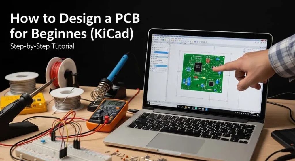
How to Design a PCB
for Beginners (KiCad)
Complete step-by-step guide from drawing your first schematic to ordering a real printed circuit board from JLCPCB for $2. Free software, real circuit case study, zero experience required.
🎓 12 Tutorials ⏱️ ~4 Weeks 🛠️ KiCad (Free) 📦 JLCPCB Ready
What You’ll Be Able to Do After This Path
- ✅ Install and navigate KiCad the industry-standard free PCB design tool
- ✅ Convert any breadboard circuit into a clean, ERC-passing schematic
- ✅ Assign correct physical footprints and avoid the #1 beginner misalignment mistake
- ✅ Place components and route copper traces without DRC errors
- ✅ Export Gerber + drill files and order from JLCPCB for as low as $2
- ✅ Understand the 5 most common PCB mistakes and avoid every one of them
What is PCB Design?
PCB design is the process of converting an electronic circuit schematic into a physical board layout where copper traces connect electronic components on a fiberglass substrate. The result is a Printed Circuit Board the green board inside every electronic device you own.
In PCB design you work in two stages: first you draw a schematic (the logical circuit), then you create a board layout (the physical arrangement of components and copper traces). Software like KiCad handles both stages for free.
Table of Contents
- What is PCB Design? (Definitions & Concepts)
- Real Case Study: 555 Timer LED Blinker PCB (Start to Finish)
- How to Install KiCad for PCB Design (Step-by-Step)
- How to Draw a PCB Schematic for Beginners
- How to Assign Footprints in KiCad (and Avoid Misalignment)
- How to Do PCB Board Layout & Trace Routing
- How to Export Gerber Files and Order from JLCPCB
- 5 PCB Design Mistakes Beginners Make (and How to Fix Them)
- All 12 Tutorials at a Glance
- Best Free PCB Design Software Comparison
- PCB Design FAQ Beginner Questions Answered
What is PCB Design? Key Concepts Explained
Before touching KiCad, you need to understand the vocabulary. Every PCB design guide assumes you know these terms here they are, clearly defined for beginners.
Schematic vs. PCB Layout What’s the Difference?
A schematic is a symbolic diagram of your circuit it shows which components connect to which, using standardized symbols. It says nothing about physical size, shape, or position. A PCB layout is the physical realization where components are physically placed and how copper traces connect their pads.
Key PCB Design Terms Glossary for Beginners
| Term | Definition | Where Used |
|---|---|---|
| Net | An electrical connection that must exist between two or more pins | Schematic & PCB |
| Footprint | The physical pad pattern on the PCB matching a component’s leads | PCB Layout |
| Trace | A copper conductor on the PCB connecting two pads | PCB Layout |
| Via | A plated drill hole connecting copper traces on different layers | PCB Layout |
| Ratsnest | Thin lines showing unrouted connections still needing traces | PCB Layout |
| Gerber | Industry-standard file format submitted to PCB manufacturers | Fabrication |
| DRC | Design Rules Check automated error detection before ordering | Verification |
| Ground Pour | A large copper area on a layer connected to GND | PCB Layout |
| Silkscreen | White ink layer printed on board showing component labels | Assembly |
| BOM | Bill of Materials complete component list for assembly | Ordering |
Schematic → ERC → Footprint Assignment → PCB Layout → Trace Routing → DRC → Gerber Export → Order. Skip any step and the result is either a broken design or a non-functional board. This path teaches every step in sequence.
555 Timer LED Blinker PCB Complete Walkthrough
This is the exact circuit built throughout this path. Real component list, real KiCad steps, real ordered board. Follow this case study and you’ll have a functioning PCB in your hands within 4 weeks.
What the Circuit Does
A 555 timer IC in astable mode blinks an LED at approximately 1 Hz (once per second). Runs on 5–9V DC. Total component cost: under $1. Board size: 40×35mm. Simple enough that every trace and connection makes sense to a beginner complex enough to cover all real PCB skills.
Bill of Materials (Exact Components Used)
| Ref | Component | Value | Package | KiCad Footprint | Cost |
|---|---|---|---|---|---|
| U1 | NE555 Timer IC | NE555P | DIP-8 | Package_DIP:DIP-8_W7.62mm | $0.10 |
| R1 | Resistor | 10 kΩ | Axial THT | Resistor_THT:R_Axial_P10.16mm_Horizontal | $0.02 |
| R2 | Resistor | 100 kΩ | Axial THT | Resistor_THT:R_Axial_P10.16mm_Horizontal | $0.02 |
| R3 | LED Resistor | 470 Ω | Axial THT | Resistor_THT:R_Axial_P10.16mm_Horizontal | $0.02 |
| C1 | Electrolytic Cap | 10 µF / 16V | Radial THT | Capacitor_THT:CP_Radial_D6.3mm_P2.50mm | $0.05 |
| C2 | Ceramic Cap (bypass) | 100 nF | Disc THT | Capacitor_THT:C_Disc_D5.0mm_W2.5mm_P5.00mm | $0.03 |
| D1 | LED (Red, 5mm) | Red | LED 5mm THT | LED_THT:LED_D5.0mm | $0.05 |
| J1 | Power Connector | 2-pin 2.54mm | Pin Header | Connector_PinHeader_2.54mm:PinHeader_1x02_P2.54mm_Vertical | $0.05 |
Schematic Diagram
PCB Board Layout Diagram
Following this exact path, a first-time PCB designer completed this board in 6 hours total. JLCPCB shipped 5 boards in 18 days via economy shipping. Total cost: $4 for 5 PCBs ($2 boards + $2 shipping). All 5 boards worked correctly on first power-up. The LED blinks at 1 Hz as designed.
How to Install KiCad for PCB Design (Step-by-Step)
KiCad is free and installs in under 10 minutes. Here is the exact process.
Step 1: Download KiCad
- Go to kicad.org → Downloads
- Select your operating system (Windows, macOS, or Linux)
- Download the latest stable release (KiCad 8.x) not the nightly build
- File size: approximately 1.5 GB on Windows including all libraries
Step 2: Full Install vs. Minimal Install
- Missing schematic symbol library
- “Symbol not found” errors mid-project
- No 3D component models
- Must manually download libraries later
- All schematic symbols included
- All PCB footprint libraries included
- 3D STEP models for 3D viewer
- Ready to design immediately
Step 3: Create Your First KiCad Project
Open KiCad → File → New Project. Create a folder called led-blinker-pcb. Name the project 555-blinker. KiCad creates three files: .kicad_pro, .kicad_sch, and .kicad_pcb. These files must always stay in the same folder never move them individually.
Pro Tip 10 Shortcuts That Save Hours
Schematic Editor: A = Add component, W = Wire, P = Power symbol, E = Edit properties, R = Rotate. PCB Editor: X = Route trace, B = Fill pours, D = Interactive DRC, Alt+3 = 3D viewer, U = Select connected track. Learn these 10 shortcuts first your design speed triples within a week.
How to Draw a PCB Schematic for Beginners
The schematic is not the PCB it is a logical map of your circuit. Every component, every connection, every net must be defined here correctly before touching the PCB layout.
Adding the 555 Timer IC in KiCad
Press A to open the symbol chooser. Type NE555 in the search box. Select it from the Timer_RTC library. Click OK, then click the canvas to place it. The 555 symbol shows all 8 labeled pins: VCC, GND, OUTPUT, TRIGGER, THRESHOLD, CONTROL, RESET, DISCHARGE.
Adding Power Symbols
Press P for the power symbol chooser. Search VCC and place it above the 555. Search GND and place it below. These are not physical components they are schematic net labels telling KiCad which net is power and which is ground. Also add a PWR_FLAG on each to pass ERC validation.
Wiring Connections
Press W to draw wires. Click on a pin endpoint (small circle), drag to another pin endpoint, click to complete. A properly connected wire produces no dangling green squares. Wire Pin 8 to VCC, Pin 1 to GND, then follow the 555 astable configuration for the timing resistors and capacitor.
A wire that visually appears connected to a pin but isn’t snapped onto its endpoint creates an unconnected net. The schematic looks fine. The PCB traces look fine. But the electrical connection doesn’t exist. Always verify with ERC this mistake has caused countless beginner boards to arrive dead on first power-up.
Running the Electrical Rules Check (ERC)
Inspect → Electrical Rules Checker → Run ERC. A clean 555 flasher schematic has zero errors. The most common ERC errors and their fixes:
| ERC Error | Cause | Fix |
|---|---|---|
| Pin unconnected | Wire doesn’t snap to pin endpoint | Delete wire, redraw carefully snapping to pin |
| Power pin not driven | Missing PWR_FLAG on VCC/GND net | Add PWR_FLAG symbol to VCC and GND |
| Net has only one pin | Wire goes nowhere dangling end | Delete the dangling wire segment |
| Duplicate references | Two components with same ref (R1, R1) | Tools → Annotate Schematic → Re-annotate |
How to Assign Footprints in KiCad (and Avoid Misalignment)
Every schematic symbol must be assigned a footprint the physical pad layout that appears on the PCB. This is where the most expensive beginner mistake happens.
A beginner used the NE555D footprint (SOIC-8, SMD, 1.27mm pitch) but physically bought the NE555P (DIP-8, through-hole, 2.54mm pitch). The board arrived from JLCPCB. Zero holes for the IC legs. The IC cannot be inserted. Board is unusable. The fix took 5 seconds check the component package code on the bag before assigning the footprint.
How to Read Component Package Codes
| Package Code | Meaning | Mount Type | Pitch | Beginner? |
|---|---|---|---|---|
| DIP-8, DIP-16 | Dual Inline Package | Through-hole | 2.54mm | Easiest |
| SOIC-8, SOIC-16 | Small Outline IC | Surface mount | 1.27mm | Intermediate |
| TSSOP-8 | Thin Shrink Small Outline | Surface mount | 0.65mm | Advanced |
| 0805 | SMD resistor/cap size | Surface mount | 2.0mm | Intermediate |
| Axial THT | Through-hole resistor | Through-hole | Various | Easiest |
Pro Tip Always Preview the Footprint Before Confirming
In the Footprint Assignment dialog, press F to open a footprint preview. Count the pads. Verify the pad spacing matches your datasheet. Check that through-hole pads have drill holes. This 30-second check prevents receiving boards where components physically cannot be mounted.
How to Do PCB Board Layout & Trace Routing (With Real Examples)
Board layout is where schematics become physical reality. Component placement strategy is more important than most beginners realize poor placement forces long, convoluted traces that degrade signal quality and increase noise.
Component Placement The 555 Blinker Example
- J1 (Power connector) at top-left board edge connectors always at edge for cable access
- U1 (555 IC) in the center it’s the circuit hub; centering minimizes trace lengths to all 8 pins
- R1, R2 adjacent to Pins 7 and 6 of the 555 timing network traces must be short
- C1 below the 555, close to Pin 2/6 short route to the timing pins it serves
- C2 directly next to Pin 8 (VCC) bypass caps must be within 3–5mm of the power pin they decouple
- D1 (LED) at the left board edge indicator LEDs visible from outside the enclosure
Trace Width Guidelines
| Net | Width | Current Capacity | Why This Width |
|---|---|---|---|
| VCC power rail | 0.5 mm | ~1A | Power traces need extra width for current and thermal reasons |
| GND | Ground pour | Unlimited | Entire B.Cu layer = GND no individual GND traces needed |
| Signal traces | 0.25 mm | ~0.5A | Signal-level currents only (milliamps) |
| LED current path | 0.25 mm | ~0.5A | Max 20mA through LED 0.25mm handles easily |
Adding the Ground Pour Don’t Skip This
Select the B.Cu layer. Go to Place → Zone. Draw a rectangle covering the full board. Set net to GND. Press B to fill all zones. The entire back copper layer becomes a solid GND plane. This eliminates the need to route individual GND traces and provides electromagnetic shielding standard professional practice on every 2-layer board.
Lower GND impedance (better noise immunity), shorter return paths for all signals, thermal mass for heat dissipation, fewer traces to manually route, and professional appearance. On the 555 blinker, using a ground pour reduces total routing work by approximately 40% and produces a cleaner board.
How to Export Gerber Files and Order from JLCPCB
After a clean DRC, generating Gerbers and ordering takes about 15 minutes total.
Exporting Gerbers from KiCad Exact Steps
- PCB Editor: File → Fabrication Outputs → Gerbers (.gbr)
- Set Output directory to
gerbers/inside your project folder - Check layers: F.Cu, B.Cu, F.Mask, B.Mask, F.Silkscreen, Edge.Cuts
- Enable “Plot reference designators” and “Plot footprint values”
- Click Plot
- Click Generate Drill Files → Generate Drill File
- Select all files in gerbers/ → Compress to ZIP
Before uploading: Open KiCad’s Gerber Viewer → load all files from gerbers/ folder. Verify copper traces present, drill holes at all pads, board outline is a closed shape, silkscreen is readable. A 5-minute review prevents ordering a $2 broken board and waiting 3 weeks to discover the problem.
JLCPCB Order Settings for Beginners
| Setting | Value for Beginners | Notes |
|---|---|---|
| Quantity | 5 pcs | Minimum order cheapest per-board cost |
| PCB color | Green | Fastest turnaround, lowest cost |
| Surface finish | HASL (lead-free) | Default fine for all beginner projects |
| PCB thickness | 1.6 mm | Standard fits all common connectors |
| Copper weight | 1 oz | Standard for signal boards under 2A |
| Shipping | Economy or DHL | Economy: 2–4 weeks / DHL: 5–7 days |
🚫 5 PCB Design Mistakes Beginners Make
These five mistakes account for over 90% of beginner PCB failures. Every single one is completely avoidable once you know what to look for.
Assigning a SOIC-8 (SMD) footprint to a DIP-8 (through-hole) IC. The board arrives, there are no holes, the component cannot be inserted. Most expensive beginner mistake for the time it wastes.
Real example: NE555P = DIP-8, through-hole. NE555D = SOIC-8, SMD. One letter suffix difference. Completely incompatible footprints. Always check the physical component package code before assigning any footprint.
A wire that visually looks connected but isn’t snapped to a pin endpoint creates an unconnected net. KiCad won’t route that connection. The board arrives with all components soldered, nothing works. Debugging this on a physical board is extremely difficult.
Submitting Gerbers with clearance violations. Two traces too close together get bridged during copper etching, creating short circuits. KiCad catches these automatically but only if you run DRC. Many beginners export Gerbers immediately after routing without checking.
Placing an LED or electrolytic capacitor footprint with wrong orientation on the silkscreen. Assembly follows the silkscreen, component goes in backwards, circuit fails. This is especially tricky because the board looks physically correct the wrong component just faces the wrong way.
Visual clue: In KiCad, the LED footprint’s square pad = Anode (+). The electrolytic cap footprint marks the + side explicitly. Verify both in the 3D viewer before ordering.
PCB fabs use a ~0.5mm wide router bit to cut the board edge. Copper traces within 0.5mm of Edge.Cuts get physically cut or exposed. Components too close to the edge get damaged during routing. Boards arrive with sliced traces along all edges.
📚 All 12 Tutorials Complete Path Overview (~4 Weeks)
Best Free PCB Design Software KiCad vs EasyEDA vs Fritzing
| Software | Cost | Platform | Best For | Biggest Problem | Verdict |
|---|---|---|---|---|---|
| KiCad 8 | Free, open-source | Win/Mac/Linux | Professional PCB design, learning proper workflow | Steeper initial learning curve | Best Choice |
| EasyEDA | Free (JLCPCB integrated) | Web-based | Quick JLCPCB orders, LCSC component sourcing | Proprietary format, internet required | Acceptable |
| Fritzing | $8 one-time | Win/Mac/Linux | Breadboard diagrams, education visuals | Not suitable for professional PCB work | Not Recommended |
| Altium Designer | ~$300/month | Windows only | Commercial professional PCB design | Extremely expensive for hobbyists | Professional Only |
| Eagle (Autodesk) | Free (limited) | Win/Mac/Linux | Was popular before KiCad improved | Free version board size limit, KiCad now better | Legacy Only |
❓ PCB Design FAQ Beginner Questions Answered
PCB design for beginners follows 7 steps: (1) Draw schematic in KiCad, (2) Run ERC and fix all errors, (3) Assign physical footprints to every component, (4) Import the netlist into PCB Editor, (5) Place components on the board, (6) Route copper traces, (7) Run DRC, export Gerbers, order from JLCPCB. A beginner can complete a simple board like the 555 blinker in approximately 4–6 hours of active work.
KiCad is the best free PCB design software for beginners. It is completely free with no feature restrictions, runs on Windows, macOS, and Linux, and exports industry-standard Gerber files accepted by all manufacturers. While EasyEDA is simpler to start, KiCad teaches proper PCB design workflow that scales to professional use. Fritzing is not recommended for actual PCB design.
Yes, KiCad is completely free. It is open-source software (GPL license) maintained by a community and supported by CERN. There is no free tier with restrictions, no premium version, and no subscription fee. The full software including all schematic symbol libraries, PCB footprint libraries, and 3D STEP models downloads and installs at zero cost. The only money you spend is on PCB fabrication itself starting at $2 on JLCPCB.
A Gerber file is the industry-standard PCB manufacturing format. Each layer of your PCB is a separate file front copper, back copper, solder mask, silkscreen, board outline. The factory uses these files to control photo-plotting, etching, drilling, and coating machines. KiCad exports all required Gerber files plus an Excellon drill file in a few clicks. You zip them together and upload to JLCPCB.
A schematic is a logical diagram showing which components connect to which using standard symbols with no physical dimensions. A PCB layout is the physical implementation: actual component footprints positioned on a board with copper traces of specific widths routing the connections. In KiCad, you work on the schematic first (Schematic Editor), then transfer connections to the PCB Editor for physical layout.
JLCPCB manufactures standard 2-layer boards in 24–48 hours. Shipping depends on your choice: economy shipping takes 2–4 weeks; DHL Express takes 5–7 business days. From Pakistan, economy shipping is typically 2–3 weeks; DHL takes 7–10 days. Total from order to boards in hand: 2–5 weeks. JLCPCB sends email updates at each manufacturing stage.
Debug in this order: (1) Visual inspection with magnifying glass look for solder bridges (excess solder connecting pads that shouldn’t be connected) and cold joints (dull, grainy solder). (2) Multimeter continuity between VCC and GND when powered off should read open circuit. If it beeps, you have a short find the solder bridge. (3) Check component polarities reversed LED, capacitor, or IC. (4) Check all IC pins properly seated in through-holes. (5) Trace each net from your KiCad schematic to the physical board. Board fabrication is almost never the cause of failure on a DRC-clean design.
No. PCB design in KiCad is entirely graphical you draw schematics visually, place components by dragging, and route traces by clicking. There is zero code involved in the PCB design process. Programming is only relevant if you want to write firmware for a microcontroller that goes on your PCB but that is a completely separate skill. This entire 4-week path contains no coding whatsoever.
⚠️ Safety & Important Notes
- Soldering iron safety: Soldering irons reach 300–400°C and cause instant burns. Always use a stable iron holder, never leave a hot iron unattended, and work in a ventilated area flux fumes irritate the respiratory system with prolonged exposure.
- Solder choice: Use rosin-core lead-free solder (Sn99.3/Cu0.7). If using leaded solder (Sn63/Pb37), wash hands thoroughly after handling and never eat or drink near your workspace.
- Voltage range: This path covers low-voltage DC circuits (3.3V–12V). Mains-voltage PCB design (110V/220V AC) requires additional safety clearances and IPC-2221 standards not covered here.
- PCB fabs manufacture exactly what Gerber files specify. A DRC-clean board with a logical schematic error will still be manufactured and shipped as-is. Always verify your schematic against your intended circuit before ordering.
- Always verify Gerber dimensions in KiCad’s built-in Gerber Viewer before upload JLCPCB’s automated preview is a secondary check, not a replacement for your own verification.
🎯 The Bottom Line
PCB design is not as complex as it appears. The workflow is a learnable, repeatable process schematic, footprints, layout, routing, export, order. KiCad gives you professional-grade tools at zero cost. JLCPCB gives you real manufactured boards for $2.
The 5 mistakes section alone will prevent the most common reasons beginner boards fail. The 555 blinker case study gives you a real circuit, real component decisions, and real layout rationale not abstract theory disconnected from practice.
Every professional PCB designer started exactly where you are right now. The $4 board you hold at the end of this path is the beginning of being able to design anything shields, sensors, motor drivers, audio amplifiers. The workflow never changes. Master it once. Use it forever.
Software references: KiCad 8.x stable. JLCPCB pricing current as of early 2026. Component prices approximate and vary by supplier.