The Periodic Table You Actually Need Elements Behind Every Circuit, Sensor & Battery
Forget memorizing atomic masses. This is the engineer’s periodic table which elements make your MOSFETs switch, your batteries charge, your LEDs glow, and your solder flow.
By an Electronics & Material Science Practitioner 12 min read
Key Takeaways
- Silicon (Si, Z=14) dominates semiconductors not because it’s the best semiconductor it’s because SiO₂ forms a near-perfect insulating oxide layer, enabling MOSFET gate fabrication that no other element matches.
- Copper (Cu) carries 96% of all PCB current with resistivity of just 1.68 × 10⁻⁸ Ω·m the only metal that beats it is silver, which costs 100× more per kg.
- Lithium (Li) powers modern batteries because it’s the lightest metal (6.94 g/mol) with the most negative electrode potential (−3.04V), giving the highest energy density of any metallic anode.
- Gallium (Ga) compounds create every LED you’ve ever used GaN for blue/white, GaAs for infrared, GaP for green/yellow. No gallium = no LED revolution.
- Rare earth elements aren’t rare Neodymium (Nd) and Samarium (Sm) are more abundant than tin, but extracting and refining them is environmentally destructive, creating geopolitical supply chain risks.
- Tin-lead solder (Sn63/Pb37) melts at 183°C and remains the gold standard for reliability lead-free alternatives (SAC305: Sn96.5/Ag3.0/Cu0.5) melt 34°C higher at 217°C, requiring more thermal stress on components.
- Gold (Au) is used on connector contacts not for conductivity but because it never oxidizes even 0.05µm of gold plating prevents contact resistance from degrading over decades.
- Tantalum (Ta) makes the best small-value capacitors because Ta₂O₅ dielectric has extremely high permittivity, allowing 100µF in a package smaller than a grain of rice.
Table of Contents
- What Is the Periodic Table (From an Engineer’s Lens)?
- Definition and Mechanism of Periodic Behavior
- Common Issues Material Failures Engineers Face
- How It Works Electron Configuration Drives Everything
- How Element Selection Reduces Circuit Failures
- Difference Between Conductor, Semiconductor & Insulator Elements
- Recommended Elements & Materials for Key Applications
- Factors Affecting Element Behavior in Circuits
- Standard Limits and Guidelines Material Specifications
- Treatment Purification, Doping & Surface Processing
- Monitoring and Follow-Up Material Degradation Tracking
- How to Make Element-Based Projects You Can Build
- Potential Risks Toxic & Hazardous Elements in Electronics
- Where to Use & Why Element Applications by Industry
- Alternatives Substitute Elements & Emerging Materials
- Visual Data Conductivity Comparison Chart
- Pro Tips from the Field
- FAQ People Also Ask
- Safety & Evidence Disclaimer
- The Bottom Line
What Is the Periodic Table (From an Engineer’s Lens)?
You already know the periodic table from school rows of boxes, atomic numbers, electron configurations. But here’s the thing: every chemistry textbook teaches it as an abstract academic concept. They never tell you that the periodic table is literally the component selection guide for the entire electronics industry.
Every resistor, capacitor, transistor, LED, battery, solder joint, and PCB trace in your projects is built from specific elements chosen for specific electrical, thermal, and chemical properties. When your solder joint cracks after thermal cycling, that’s a periodic table problem. When your MOSFET switches in 10 nanoseconds, that’s a periodic table achievement. When your LiPo battery swells and catches fire, that’s periodic table chemistry going dangerously wrong.
Most “periodic table” articles online regurgitate the same information: 118 elements, organized by atomic number, grouped by chemical properties. Google already shows you that in a knowledge panel. That’s not what this guide does.
This guide answers the question no textbook addresses: “Which elements actually matter for electronics engineering, what do they do in my circuits, and why should I care about their atomic-level properties when I’m just trying to get a board working?”
- You’re an electronics engineer or hobbyist who wants to understand WHY specific materials are chosen for specific components
- You’re a PCB designer wondering why copper thickness matters and what ENIG vs. HASL finish actually means chemically
- You’re an embedded systems developer who keeps hearing about “silicon vs. GaN” or “lead-free vs. leaded” without understanding the material science
- You’re a student preparing for engineering exams who needs the practical context that textbooks completely skip
- You’re sourcing components and want to understand why certain materials cost more and whether cheaper alternatives actually work
Definition and Mechanism of Periodic Behavior
The Engineering Definition
The periodic table is a systematic arrangement of 118 confirmed elements organized by increasing atomic number (Z) the number of protons in the nucleus. Elements in the same column (group) share the same number of valence electrons, which directly determines their electrical conductivity, bonding behavior, and how they interact in circuits.
For engineers, the critical insight is this: an element’s position in the periodic table tells you whether it will conduct, insulate, or semiconductor. Period.
ρ = m / (n × e² × τ)
- ρ = resistivity (Ω·m) how much the material resists current
- n = free electron density (electrons/m³) determined by valence shell configuration
- e = electron charge = 1.602 × 10⁻¹⁹ C
- τ = mean free time between collisions
- m = electron mass = 9.109 × 10⁻³¹ kg
Worked Example: Copper (Cu) has n ≈ 8.5 × 10²⁸ free electrons/m³ (one per atom, from the 4s¹ valence shell). Plugging in τ ≈ 2.5 × 10⁻¹⁴ s, you get ρ ≈ 1.68 × 10⁻⁸ Ω·m. That’s why 1 oz copper on a PCB (35µm thick, 1mm wide trace) has only ~0.48Ω per meter enough to carry amps with minimal voltage drop.
Why Elements Show Periodic Properties
- Electron shells fill in a specific order (1s, 2s, 2p, 3s, 3p, 4s, 3d, 4p…). When a new shell starts filling, properties “reset” this creates the periods (rows).
- Elements with similar valence configurations behave similarly. Group 11 (Cu, Ag, Au) all have one s-electron above a filled d-shell giving them excellent conductivity and corrosion resistance. That’s why all three are used in electrical contacts.
- Band gap energy varies predictably across the table. Group 14 elements (C, Si, Ge, Sn, Pb) go from insulator (diamond: 5.5 eV) to semiconductor (Si: 1.12 eV, Ge: 0.67 eV) to metal (Sn, Pb) as you move down because larger atoms have smaller band gaps.
Pro Tip The Band Gap Sweet Spot
Silicon’s 1.12 eV band gap at 300K isn’t the best for every application. For high-speed circuits, Gallium Arsenide (GaAs, 1.42 eV) wins because higher electron mobility means faster switching. For power electronics, Silicon Carbide (SiC, 3.26 eV) and Gallium Nitride (GaN, 3.4 eV) win because wider band gaps handle higher voltages and temperatures before breakdown. The periodic table literally maps your semiconductor options by group III-V compounds (GaAs, GaN, InP) sit in Groups 13-15, while silicon sits alone in Group 14. That’s not a coincidence it’s electron configuration geometry.
Common Issues Material Failures Engineers Face
These aren’t textbook problems these are the failures I’ve personally encountered or debugged on real boards, all traceable to element-level material behavior.
Issue #1: Tin Whisker Growth on Lead-Free Solder Joints
Pure tin (Sn) grows microscopic metallic “whiskers” over time needle-like crystalline structures that can reach several millimeters and short adjacent pins. The RoHS directive pushed the industry to lead-free solder, but removing lead (Pb) removed the alloy’s natural whisker suppression. I’ve seen tin whiskers short TQFP pins on boards that worked perfectly for 18 months. Adding 2-3% bismuth (Bi) or using conformal coating mitigates this.
Issue #2: Copper Migration Under Bias (Electrochemical Migration)
When you have two copper traces close together with a voltage difference and even trace moisture (humidity >60% RH), copper ions dissolve from the anode trace and deposit on the cathode trace as dendrites. I’ve debugged boards where a 0.15mm trace gap shorted after 6 months in a humid environment. The fix: proper conformal coating and adequate trace spacing per IPC-2221 guidelines (minimum 0.1mm for <15V, much more for higher voltages).
Issue #3: Aluminum Electrolytic Capacitor Dry-Out
Aluminum electrolytics contain a liquid electrolyte (ethylene glycol-based) that slowly evaporates through the rubber seal. The aluminum oxide (Al₂O₃) dielectric layer is fine it’s the electrolyte loss that kills them. After 5,000-10,000 hours at 105°C (or 40,000+ hours at 40°C), capacitance drops by 20%+ and ESR skyrockets. This is why power supply caps fail first. I replace electrolytics preventively in any critical system older than 7 years.
Issue #4: Gold Embrittlement in Solder Joints
When you solder to gold-plated pads (ENIG finish), the gold dissolves into the solder and forms Au-Sn intermetallics (AuSn₄). If gold content exceeds 3-5% by weight in the joint, the intermetallic phase makes the solder joint brittle it’ll crack under thermal cycling or mechanical stress. This is why ENIG pads have very thin gold (0.05-0.1µm) over nickel just enough to prevent oxidation, thin enough to dissolve harmlessly.
Silver migration on a high-impedance sensor board. A client used silver-loaded conductive epoxy near a 10MΩ impedance measurement trace. Over 3 months, silver ions migrated under bias, creating a 2MΩ parasitic path that corrupted every reading. The board looked perfect under visual inspection we only found it with a confocal microscope. Silver is an excellent conductor, but it’s the most migration-prone metal in electronics. Use it carefully in high-impedance or high-humidity applications.
Issue #5: Silicon Junction Temperature Runaway
Silicon’s intrinsic carrier concentration doubles roughly every 11°C. Above ~150°C, the intrinsic carriers overwhelm the doping concentration and the device essentially becomes a conductor this is thermal runaway. It’s why standard silicon MOSFETs are rated to 150°C or 175°C junction temperature. SiC devices handle 200°C+ because the wider band gap keeps intrinsic carriers negligible until much higher temperatures.
Issue #6: Nickel Barrier Layer Corrosion (Black Pad Defect)
In ENIG PCB finish, the electroless nickel layer can develop “black pad” a phosphorus-rich corrosion layer at the nickel surface that prevents proper solder wetting. You’ll see gray or black non-wetting patches on pads during reflow. It’s caused by aggressive immersion gold chemistry attacking the nickel. I’ve rejected entire board batches due to this. The fix is on the PCB fabricator’s side proper bath chemistry control and nickel phosphorus content (8-12% P is the sweet spot).
How It Works Electron Configuration Drives Everything
Stage 1: Valence Electrons Determine Conductivity Category
The number and binding energy of valence electrons directly control whether an element is a conductor, semiconductor, or insulator. Metals in Groups 1-3 and 11-12 have 1-3 loosely bound valence electrons in overlapping energy bands they conduct freely. Elements in Groups 14-16 with moderate band gaps (0.5-3.5 eV) are semiconductors. Elements forming covalent or ionic crystals with large band gaps (>3.5 eV) are insulators.
Stage 2: Crystal Structure Sets Mechanical Properties
Copper crystallizes in FCC (face-centered cubic) structure that’s why it’s ductile enough to draw into wire. Tungsten is BCC (body-centered cubic) harder, higher melting point (3422°C, the highest of any metal), perfect for filaments and rocket nozzles. Silicon forms diamond cubic hard, brittle, but perfect for cutting into wafers with atomically flat surfaces.
Stage 3: Electronegativity Drives Chemical Behavior
Electronegativity (tendency to attract electrons) increases going right and up in the periodic table. Fluorine (3.98) and Oxygen (3.44) are the most electronegative that’s why nearly everything oxidizes. Gold’s electronegativity (2.54) is high for a metal, which is why it resists oxidation and corrosion. Copper (1.90) sits lower it DOES oxidize, forming CuO and Cu₂O, which is why exposed copper traces tarnish and need surface finish protection.
PCB surface finishes exist because bare copper oxidizes. HASL (Hot Air Solder Leveling) coats copper with tin-lead or SAC alloy. ENIG deposits nickel (prevents copper diffusion) + gold (prevents nickel oxidation). OSP (Organic Solderability Preservative) uses an organic compound to temporarily block oxidation. Each finish uses different elements from the periodic table, and each has trade-offs in shelf life, solderability, wire bondability, and cost. Understanding the chemistry helps you choose correctly.
Stage 4: Doping Transforms Semiconductors
Pure silicon has a resistivity of ~2300 Ω·m nearly useless for circuits. But add 1 atom of phosphorus (Group 15, 5 valence electrons) per million silicon atoms and resistivity drops to ~0.05 Ω·m a 46,000× improvement. That extra electron from phosphorus is free to conduct (n-type doping). Add boron (Group 13, 3 valence electrons) instead and you create a “hole” a missing electron that acts as a positive charge carrier (p-type doping). The entire semiconductor industry every transistor, diode, and IC exists because Group 14 silicon can be precisely doped with Group 13 and Group 15 elements.
Stage 5: Compound Formation Creates New Properties
Single elements are useful, but compound formation unlocks properties no single element has. Gallium (Group 13) + Nitrogen (Group 15) = GaN a wide-bandgap semiconductor revolutionizing power electronics and LEDs. Indium + Tin + Oxygen = ITO a transparent conductor used in every touchscreen. Lead + Zirconium + Titanium + Oxygen = PZT the piezoelectric material in every ultrasonic sensor and buzzer. The periodic table isn’t just about elements it’s a recipe book for materials engineering.
Pro Tip The III-V Compound Rule
Almost every high-performance optoelectronic device uses III-V compounds elements from Group 13 (III: Al, Ga, In) combined with Group 15 (V: N, P, As). Why? Because III-V compounds have direct band gaps, meaning electrons can emit photons efficiently when transitioning between energy bands. Silicon has an indirect band gap electrons need phonon assistance to emit light, making silicon LEDs absurdly inefficient (~0.001% vs. ~50% for GaN). This is why silicon dominates computing but III-V dominates optics. Every LED, laser diode, solar cell (high-efficiency type), and photodetector uses III-V materials.
How Element Selection Reduces Circuit Failures
Choosing the right material element isn’t academic it directly impacts reliability, efficiency, and lifespan of every circuit you build.
Copper vs. Aluminum Traces Reducing Resistive Losses
Copper’s resistivity (1.68 × 10⁻⁸ Ω·m) is 40% lower than aluminum (2.82 × 10⁻⁸ Ω·m). For a 10cm PCB trace carrying 2A, switching from aluminum to copper reduces I²R losses by 40%. Over millions of traces in a data center, this translates to megawatts of saved energy. That’s why PCBs use copper even though aluminum is 70% cheaper per kg.
GaN vs. Silicon Reducing Switching Losses
GaN power transistors (like the EPC2036 or GaN Systems GS66508T) switch 10× faster than equivalent silicon MOSFETs because GaN’s electron mobility in a 2DEG (two-dimensional electron gas) structure reaches ~2000 cm²/V·s vs. silicon’s ~1400 cm²/V·s. Faster switching = less time in the lossy transition region = less heat. A 100W USB-C PD charger using GaN achieves 94% efficiency in a package half the size of a silicon-based design.
Tantalum vs. Aluminum Capacitors Reducing Size by 80%
Tantalum pentoxide (Ta₂O₅) has a dielectric constant of ~25 vs. aluminum oxide (Al₂O₃) at ~9. That means a tantalum capacitor achieves the same capacitance in 60-80% less volume. A 100µF tantalum polymer cap (like the Kemet T520) fits in a 7343 case (7.3mm × 4.3mm) try getting 100µF aluminum electrolytic anywhere near that size.
- Copper over aluminum: 40% lower trace resistance → less voltage drop, less heat
- GaN over silicon: 10× faster switching → 3-5% higher converter efficiency
- Tantalum over aluminum caps: 60-80% volume reduction → denser board layout
- Gold contacts over tin: Contact resistance stable for 20+ years vs. 3-5 years before oxidation degradation
- SiC over silicon diodes: Near-zero reverse recovery → eliminates shoot-through losses in bridge circuits
Difference Between Conductor, Semiconductor & Insulator Elements
| Property | Conductors | Semiconductors | Insulators |
|---|---|---|---|
| Band Gap | 0 eV (overlapping bands) | 0.1 – 3.5 eV | >3.5 eV |
| Resistivity (Ω·m) | 10⁻⁸ to 10⁻⁶ | 10⁻⁴ to 10⁶ | 10⁸ to 10¹⁸ |
| Key Elements | Cu, Ag, Au, Al, W | Si, Ge, GaAs, GaN, SiC | SiO₂, Al₂O₃, Diamond |
| Temp Effect on Resistance | Increases with temp (+PTC) | Decreases with temp (−NTC) | Decreases slightly at extreme temp |
| Free Carriers at 300K | ~10²⁸ – 10²⁹ /m³ | ~10¹⁰ – 10¹⁹ /m³ | ~0 – 10⁷ /m³ |
| Controllable? | No (always conducts) | Yes (doping, voltage, light) | No (always insulates) |
| Use in Circuits | Traces, wires, contacts | Transistors, diodes, ICs | Insulation, dielectrics, substrates |
Recommended Elements & Materials for Key Applications
| Application | Best Element/Material | Key Property | Cost Level | Quality | Specific Product |
|---|---|---|---|---|---|
| PCB Traces | Copper (Cu) | ρ = 1.68×10⁻⁸ Ω·m | $8-10/kg | Gold Standard | 1oz (35µm) ED copper foil |
| IC Semiconductor | Silicon (Si) | Band gap 1.12 eV, perfect oxide | $30-50/wafer | Industry Standard | CZ-grown 300mm wafers |
| LEDs (Blue/White) | GaN / InGaN | Direct band gap 3.4 eV | $0.02-0.50/die | Excellent | Cree XP-E2, Lumileds LUXEON |
| Battery Anode | Lithium (Li) / Graphite (C) | −3.04V electrode potential | $15-25/kg (Li₂CO₃) | Dominant | Samsung SDI, LG Chem cells |
| Solder (Reliable) | Sn63/Pb37 | Eutectic 183°C, excellent flow | $25-40/kg | Best Reliability | Kester 44, Multicore 362 |
| Solder (Lead-Free) | SAC305 (Sn96.5/Ag3/Cu0.5) | RoHS compliant, 217-220°C | $35-60/kg | Good | Kester K100LD, Indium 3.2HF |
| Permanent Magnets | Neodymium (NdFeB) | BHmax up to 52 MGOe | $50-200/kg | Strongest Available | N52 grade sintered NdFeB |
Factors Affecting Element Behavior in Circuits
Factor 1: Temperature
Temperature changes everything. Copper’s resistivity increases ~0.4% per °C (positive temperature coefficient). Silicon’s intrinsic carrier concentration doubles every ~11°C. Solder creep rate follows an Arrhenius relationship doubling roughly every 10°C increase. A PCB operating at 85°C ages approximately 8× faster than one at 25°C for material degradation purposes.
Factor 2: Purity Level
Electronic-grade silicon must be 99.9999999% pure (9N) one impurity atom per billion silicon atoms. Even 99.99% (4N) silicon is useless for ICs because uncontrolled impurities create unpredictable carrier concentrations. Copper for PCBs needs 99.9%+ purity. Lower purity = higher resistivity = more heat = more problems.
Factor 3: Crystal Orientation
Silicon wafers are specified by crystal orientation (100), (110), or (111). Most CMOS uses (100) orientation because it has the lowest surface state density at the Si/SiO₂ interface, giving the best MOSFET performance. MEMS devices sometimes use (110) because it etches anisotropically in KOH, creating vertical sidewalls. Same element, same purity but crystal orientation changes the electrical behavior.
Factor 4: Oxidation State
Copper is great as Cu⁰ (metallic). As Cu₂O (cuprous oxide) it becomes a p-type semiconductor historically used in rectifiers before silicon. As CuO (cupric oxide) it’s a poor conductor. When your copper trace oxidizes, the contact resistance can increase 100× at the oxidized interface. This is why solderability degrades on bare copper boards stored without protective finish for more than 2 weeks.
Electrolytic capacitor lifetime follows the Arrhenius 10°C rule: for every 10°C above the rated temperature, lifetime halves. A 105°C-rated cap at 85°C lasts 4× longer than at 105°C. At 65°C, it lasts 16× longer. This means a cap rated 2,000 hours at 105°C actually lasts 32,000 hours at 65°C roughly 3.6 years of continuous operation. Place your electrolytics away from hot components (voltage regulators, power MOSFETs) and you’ll dramatically extend board lifespan.
Factor 5: Mechanical Stress
Piezoelectric elements (quartz SiO₂, PZT Pb(Zr,Ti)O₃) generate voltage under mechanical stress. But even non-piezoelectric materials are affected: resistor values shift under strain (strain gauge principle), solder joints crack under thermal cycling stress, and semiconductor die can exhibit piezoresistive shifts in current when mechanically stressed by packaging.
Factor 6: Radiation Exposure
Radiation creates electron-hole pairs in semiconductors, causing latch-up in CMOS (potentially destructive), bit-flips in SRAM (single-event upsets), and threshold voltage shifts in MOSFETs. Space-grade components use radiation-hardened processes often silicon-on-insulator (SOI) substrates or specialized layout techniques. Even terrestrial electronics at high altitudes experience higher neutron flux from cosmic rays one reason data centers at altitude have higher soft error rates.
Standard Limits and Guidelines Material Specifications
| Parameter | Standard | Limit / Specification | Why It Matters |
|---|---|---|---|
| Lead (Pb) in electronics | EU RoHS (2011/65/EU) | <1000 ppm (0.1% by weight) | Restricts leaded solder in consumer products |
| Cadmium (Cd) | EU RoHS | <100 ppm (0.01%) | Toxic; was used in NiCd batteries, now restricted |
| Mercury (Hg) | EU RoHS | <1000 ppm (0.1%) | Was used in switches, relays, backlights |
| Copper purity for PCB | IPC-4562A | ≥99.8% Cu (ED Grade 1) | Ensures consistent resistivity and etching behavior |
| Silicon wafer purity | SEMI M1 | ≥9N (99.9999999%) | Uncontrolled impurities destroy transistor yield |
| Solder alloy composition | J-STD-006C | SAC305: Sn96.5±0.5/Ag3.0±0.3/Cu0.5±0.2 | Tight composition control for consistent melting behavior |
| Conflict minerals | Dodd-Frank Act §1502 | Must disclose Ta, Sn, W, Au sourcing | Tantalum, tin, tungsten, gold from DRC conflict zones |
RoHS has critical exemptions: high-temperature lead solder (>85% Pb content, like Pb90Sn10 used in die-attach) is still allowed. Lead in glass (CRTs, certain sensors) is exempt. Lead in ceramic capacitors (PZT-based piezoelectric ceramics) is exempt. Military and aerospace electronics can use leaded solder under MIL-STD specifications. If you’re designing for an exempt category, you can still use leaded components and often should, for reliability.
Treatment Purification, Doping & Surface Processing
Silicon Purification: From Sand to 9N Purity
- Reduction: SiO₂ (quartz sand) + Carbon → Si (metallurgical grade, ~98-99% pure) at 1700°C in an electric arc furnace
- Siemens Process: Si + HCl → SiHCl₃ (trichlorosilane) → distillation to remove impurities → CVD deposition: SiHCl₃ + H₂ → Si (polycrystalline, 9N+ pure)
- Czochralski Growth: Melt the polysilicon at 1414°C, dip a seed crystal, slowly pull upward while rotating → single crystal ingot (300mm diameter, 1-2m long)
- Wafering: Diamond wire saw cuts ingot into ~775µm thick wafers → lapping → polishing to <0.5nm surface roughness
Doping Methods
- Ion Implantation: Accelerate dopant ions (B⁺, P⁺, As⁺) to 10-200 keV and shoot them into the wafer surface. Precise depth and concentration control. Used for all modern IC fabrication.
- Diffusion: Expose wafer to dopant gas (PH₃, B₂H₆) at 900-1100°C. Dopant atoms diffuse into silicon. Older technique, still used for deep junctions and solar cells.
- Epitaxial Growth: Grow a thin doped silicon layer on top of the wafer via CVD. Creates sharp doping transitions impossible with diffusion.
PCB Surface Finishes Element-Level Choices
- HASL (Sn/Pb or SAC): Hot molten solder dipped onto copper. Cheap, excellent solderability, but uneven surface unsuitable for fine-pitch (<0.5mm) components.
- ENIG (Ni/Au): Electroless nickel (3-6µm) + immersion gold (0.05-0.1µm). Flat surface, good for BGA/fine-pitch. Gold prevents nickel oxidation. Most popular for production boards.
- Immersion Tin: Pure tin layer over copper. Flat, good solderability, but limited shelf life (~6 months) due to tin whisker risk and intermetallic growth.
- Immersion Silver: Thin silver layer. Excellent solderability, but tarnishes in sulfur-containing environments and has migration risk.
- OSP (Organic): Organic compound layer. Cheapest, flattest, but single-reflow only can’t survive multiple solder passes.
Pro Tip Choosing PCB Finish by Application
For prototyping and hand soldering, HASL (leaded) is king the thick solder layer is forgiving and easy to work with. For production BGA boards, ENIG is the standard. For RF/microwave circuits, immersion silver provides the lowest signal loss (silver has the highest conductivity of any element). For ultra-low-cost consumer boards with single-pass reflow, OSP saves money. I default to ENIG for anything going to production the slight cost premium (usually +$3-5 per board) is worth the reliability and rework tolerance.
Monitoring and Follow-Up Material Degradation Tracking
Monitor 1: Solder Joint Integrity (Visual + X-Ray)
After reflow, inspect solder joints for proper wetting, fillet formation, and absence of voids. For BGA packages, X-ray inspection (using a Dage or Nordson system) is mandatory you literally cannot see BGA joints. Look for: voids >25% of pad area, bridging, head-on-pillow defects, and non-wetting. For long-term monitoring, thermal cycling tests (IPC-9701: -40°C to +125°C, 2000 cycles) reveal early fatigue failures.
Monitor 2: Copper Trace Resistance
Use a 4-wire (Kelvin) measurement to check trace resistance. A 1oz copper trace 10mm long, 0.25mm wide should measure approximately 0.019Ω at 25°C. If you measure significantly higher, suspect under-etched copper (thinner than specified), micro-cracks, or corrosion. Repeat the measurement at regular intervals during accelerated aging to track degradation.
Monitor 3: Capacitor ESR Trending
Measure electrolytic capacitor ESR monthly using an ESR meter (like the Peak Atlas ESR70 or DE-5000 LCR meter at 100kHz). A new 100µF/25V aluminum electrolytic typically measures 0.1-0.5Ω ESR. When ESR exceeds 3× the initial value, the cap is approaching end-of-life. Plot the ESR trend a suddenly accelerating curve means failure is imminent.
Monitor 4: Contact Resistance on Connectors
Gold-plated contacts should maintain <20mΩ contact resistance for the connector's rated lifecycle (typically 500-1000 insertions). Tin-plated contacts start around 10-50mΩ but can degrade to 500mΩ+ as the thin tin oxide layer builds up. If you're seeing intermittent issues on tin-plated connectors, measure contact resistance with a micro-ohmmeter it often reveals the problem before complete failure.
- Electrolytic capacitors: After 7-10 years of continuous operation, or when ESR exceeds 2× datasheet value
- Tin-plated connectors: After 50-70% of rated insertion cycles, or when contact resistance exceeds 100mΩ
- Thermal interface material: Every 3-5 years thermal paste (typically silicone + ZnO or Al₂O₃ filler) dries out and thermal resistance increases
- Battery cells: When capacity drops below 80% of original (typically after 300-500 full cycles for LiPo)
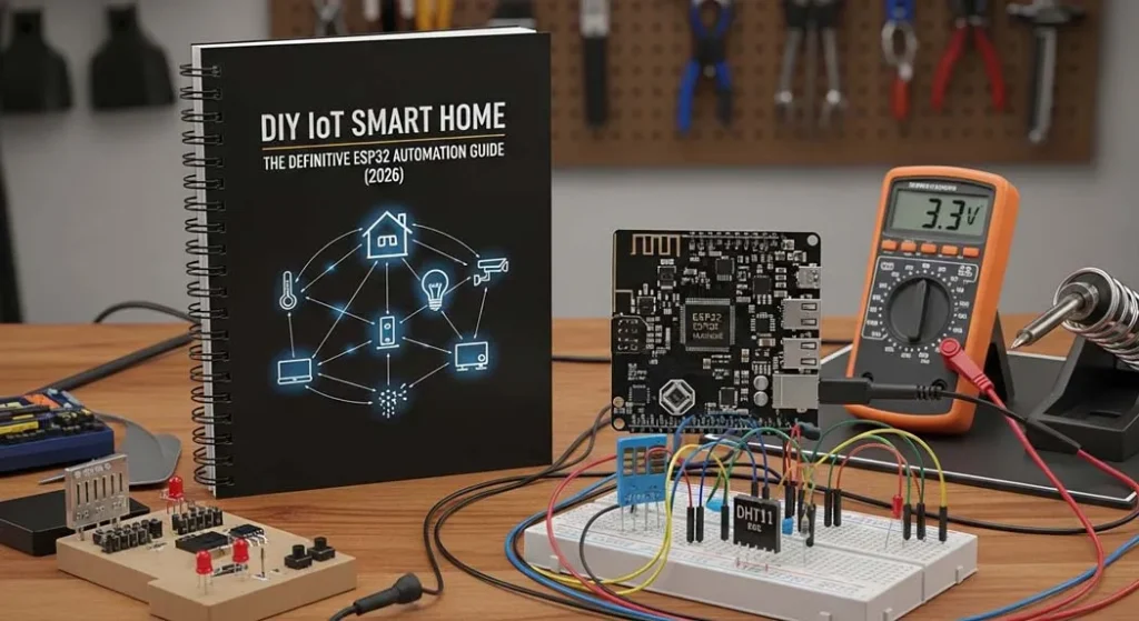
How to Make An Element-Based Sensor Project
Let’s build a thermocouple temperature sensor a device that directly exploits the Seebeck effect between two different metallic elements to measure temperature. No IC, no ADC calibration headaches pure periodic table physics.
Materials List
- Type K thermocouple wire: Chromel (Ni-Cr alloy) + Alumel (Ni-Al alloy) $3-8 for 1 meter pair
- AD8495 thermocouple amplifier module (or MAX31855 for SPI digital output) $5-12
- Arduino Uno or ESP32 for reading the output
- Breadboard, jumper wires, multimeter for verification
- Heat source for testing (soldering iron tip works perfectly)
Step-by-Step Build
- Strip the thermocouple wires: You’ll see two wires yellow (Chromel, positive) and red (Alumel, negative). Strip 10mm of insulation from both ends of each wire.
- Create the sensing junction: Twist the stripped ends of both wires together tightly. For best results, weld them using a TIG welder or twist and solder (though soldering introduces a third metal use high-temp silver solder if needed).
- Connect to AD8495: Connect Chromel (yellow) to the “+” input and Alumel (red) to the “−” input. The AD8495 provides cold-junction compensation internally and outputs 5mV/°C so 25°C reads as 125mV, 100°C reads as 500mV.
- Wire to Arduino: Connect AD8495 output to Arduino A0. VCC to 5V, GND to GND. Add a 0.1µF ceramic capacitor across VCC and GND close to the AD8495.
- Upload code: Read A0 with analogRead(), convert: Temperature = (analogRead(A0) * 5000.0 / 1024.0) / 5.0 for °C.
- Calibrate: Verify against a known temperature ice water (0°C) and boiling water (100°C at sea level, adjust for altitude).
- Test range: Type K handles −200°C to +1350°C. The AD8495 limits you to approximately −25°C to +400°C in the default gain configuration.
The thermocouple sensing tip will be at whatever temperature you’re measuring. At 300°C+ (oven, exhaust, soldering iron tip), the wire is a burn hazard. Use fiberglass or ceramic insulated thermocouple wire for temperatures above 200°C standard PVC insulation melts at ~80°C. Never grab a thermocouple wire that’s been in contact with a heat source without verifying it has cooled.
Pro Tip Why Two Different Metals?
The Seebeck effect generates a voltage proportional to the temperature difference between two junctions of dissimilar metals. Using TWO different metals is essential same-metal junctions produce zero net voltage. Type K (Chromel/Alumel) generates approximately 41µV/°C. Type T (Copper/Constantan) generates ~43µV/°C but only works to 400°C. Type S (Platinum/Platinum-Rhodium) handles 1750°C but generates only ~10µV/°C and costs vastly more. The periodic table directly determines which element combinations produce the highest Seebeck coefficients.
Potential Risks Toxic & Hazardous Elements in Electronics
Risk 1: Lead (Pb) Neurotoxin
Lead solder (Sn63/Pb37) is still widely used in hobbyist and aerospace electronics. Lead is a cumulative neurotoxin no safe exposure level exists. Always wash hands after soldering with leaded solder. Don’t eat or drink at your soldering station. Lead fumes during soldering are minimal (solder temperature of ~370°C is well below lead’s boiling point of 1749°C), but the flux fumes ARE irritating use ventilation.
Risk 2: Cadmium (Cd) Carcinogen
Found in older NiCd batteries, some CdS photoresistors, and CdSe quantum dots. Cadmium is a known carcinogen (Group 1, IARC). Never incinerate NiCd batteries cadmium vaporizes and becomes airborne. The LDR (light-dependent resistor) on your bench may contain CdS handle with care and don’t grind or sand it.
Risk 3: Beryllium (Be) Lung Disease
Beryllium copper (BeCu) alloys are used in high-reliability connectors, springs, and RF shielding due to excellent fatigue resistance and conductivity. Beryllium dust causes chronic beryllium disease (CBD) a progressive, incurable lung condition. Never sand, grind, or machine BeCu parts without proper respiratory protection. Pre-formed BeCu springs in sealed connectors pose no handling risk in normal use.
Risk 4: Lithium (Li) Fire & Explosion
Metallic lithium reacts violently with water and burns at extreme temperatures. LiPo and Li-ion cells contain flammable organic electrolytes. A punctured, overcharged, or short-circuited cell can undergo thermal runaway reaching 500°C+ with venting of toxic fluorine compounds. I’ve personally witnessed a LiPo cell vent with flames during a charging test. Always use proper BMS (Battery Management System), charge in a fireproof bag, and never leave charging batteries unattended.
Gallium Arsenide (GaAs) wafers and chips contain arsenic a potent toxin and carcinogen. Intact GaAs devices (packaged ICs) pose no handling risk. But if you’re doing research-level work with bare GaAs wafers dicing, lapping, etching arsenic dust and arsine gas (AsH₃, lethal at 150-300 ppm) are serious hazards requiring fume hoods, gloves, and respiratory protection. Most hobbyists will never encounter bare GaAs, but if you’re breaking open old microwave diodes or photodetectors, be aware.
Risk 5: Mercury (Hg) Neurotoxin, Bioaccumulative
Mercury was used in tilt switches, thermostats, mercury-wetted relays, and CCFL backlight tubes (in pre-LED monitors and TVs). A broken CCFL tube releases mercury vapor ventilate the area and don’t vacuum it (that disperses the droplets). Modern electronics have largely eliminated mercury, but legacy equipment disassembly requires awareness.
Where to Use & Why Element Applications by Industry
Consumer Electronics
Silicon for all processors and memory. GaN in fast chargers (Anker Nano, Apple 35W). OLED displays use organic compounds with iridium (Ir) complexes for phosphorescent emission. Gorilla Glass contains aluminum (Al) ions exchanged with potassium (K) for surface hardness (ion exchange strengthening). Every element choice directly impacts the product’s performance.
Automotive
SiC MOSFETs (Wolfspeed C3M series, Infineon CoolSiC) in EV traction inverters handling 400-800V bus voltages at 200°C junction temperatures that silicon can’t survive. NdFeB permanent magnets in EV motors (Tesla Model 3 uses ~1kg of rare earths per motor). Platinum (Pt) and Palladium (Pd) in catalytic converters approximately 3-7g per vehicle, worth $100-300 in precious metals.
Aerospace & Defense
Radiation-hardened silicon-on-insulator (SOI) for space-grade processors. Titanium (Ti) for structural components 45% lighter than steel with comparable strength and excellent corrosion resistance. Tungsten (W) for radiation shielding and kinetic penetrators (density 19.3 g/cm³ vs. lead’s 11.3). Gallium Arsenide (GaAs) for space solar cells 28-30% efficiency vs. silicon’s 20-22%.
Medical Devices
Titanium for implants (hip joints, dental, pacemaker casings) biocompatible and corrosion-resistant in body fluids. Platinum-iridium (Pt-Ir) for pacemaker electrodes stable, non-reactive, low impedance in body tissue. Technetium-99m (Tc) the most-used medical radioisotope for diagnostic imaging (gamma cameras).
Renewable Energy
Silicon dominates solar cells (>95% of market) monocrystalline PERC cells reach 22-24% efficiency. Cadmium Telluride (CdTe) for thin-film solar cheaper, lower efficiency (~18%), but less energy-intensive to manufacture. Neodymium in wind turbine generators a single 3MW offshore turbine contains approximately 600kg of NdFeB magnets.
Pro Tip Emerging Application: Perovskite Solar Cells
Perovskite solar cells use compounds with the ABX₃ crystal structure typically methylammonium lead iodide (CH₃NH₃PbI₃). Lab efficiency has reached 33.7% in tandem with silicon (2024 record). The lead (Pb) content is a concern, but the amount per square meter is ~0.4g far less than the lead in a car battery. Watch this space perovskite/silicon tandems could reach 35%+ commercial efficiency by 2028, fundamentally changing the solar industry.
Alternatives Substitute Elements & Emerging Materials
| Current Standard | Alternative | Advantage | Disadvantage | Maturity | Best When |
|---|---|---|---|---|---|
| Silicon (Si) | GaN, SiC | Higher voltage, temp, speed | 3-5× cost, less mature ecosystem | Production Ready | High-power, high-freq, high-temp |
| Copper (Cu) traces | Silver nanoparticle ink | Printable, flexible substrates | Higher resistivity, migration risk | Emerging | Printed/flexible electronics |
| NdFeB magnets | Ferrite, SmCo, non-RE motors | No rare earth supply risk | 30-60% weaker magnetic field | Available Now | When supply chain risk > performance |
| Lithium-ion batteries | Sodium-ion (Na-ion) | Abundant Na, no lithium needed | ~30% lower energy density | Early Production | Stationary storage, low-cost EVs |
| ITO (In₂O₃:Sn) touchscreens | Silver nanowire, graphene, PEDOT:PSS | No rare indium dependency | Durability, uniformity challenges | R&D to Early Production | Large-area flexible displays |
| Lead solder (Sn/Pb) | SAC305, SnBi, SnCu | RoHS compliant | Higher melt temp, tin whisker risk | Industry Standard | Any RoHS-regulated product |
📊 Electrical Conductivity of Key Engineering Elements
(Relative to Silver = 100%)
🔧 Pro Tips from the Field
Tip #1 Copper Weight on PCBs Is Not What You Think
“1 oz copper” doesn’t mean your trace weighs 1 ounce. It means if you took one square foot of the copper foil, it would weigh 1 ounce corresponding to a thickness of 35µm (1.4 mil). 2 oz = 70µm. For high-current traces, I’ve used 3 oz (105µm) copper on power supply boards. But heavier copper is harder to etch precisely fine-pitch traces below 0.15mm become unreliable on 2oz+ copper. Match copper weight to your current AND trace width requirements, not just one parameter.
Tip #2 Gold Plating Thickness Matters Enormously
For edge connectors (like PCIe slots, memory DIMM), gold plating must be hard gold at 0.75-1.25µm thickness (per IPC-4556) this survives hundreds of insertion cycles. For soldering-only ENIG pads, gold is only 0.05-0.1µm. If you accidentally order hard gold thickness on solder pads, you’ll get gold embrittlement in every joint. I’ve seen this mistake cost a company $40,000 in rework. Always specify different gold thicknesses for connector fingers vs. solder pads on the same board.
Tip #3 Aluminum Electrolytic Caps Near Hot Components = Guaranteed Failure
I’ve debugged hundreds of power supply failures. The #1 root cause: electrolytic capacitors placed within 10mm of voltage regulators or power MOSFETs. The cap’s electrolyte evaporates faster at elevated temperatures, and the 10°C doubling rule means a cap running at 95°C dies 4× faster than one at 75°C. My rule: always place electrolytics on the OPPOSITE side of the board from heat sources, or use ceramic/polymer caps in hot zones.
Tip #4 Solder Paste Expiration Is Real
Solder paste (SAC305 or Sn63/Pb37) has a 6-month shelf life when refrigerated at 0-10°C. The flux activators degrade over time, and the spherical solder particles oxidize. Expired paste causes poor wetting, solder balls, and voids. I once spent two days debugging reflow defects before discovering the solder paste was 8 months past expiration. Always check the expiration date, and bring paste to room temperature for 2-4 hours before use cold paste doesn’t print properly through stencil apertures.
Tip #5 The Specific Resistance of Your Solder Joint
A well-formed SAC305 solder joint has a bulk resistivity of approximately 1.3 × 10⁻⁷ Ω·m about 8× higher than copper. For signal traces, this is negligible. But for high-current paths (>5A), solder joint resistance contributes measurable voltage drop and heating. On a motor driver board, I measured 15mV drop across a single solder joint at 8A small, but with 20 joints in series on a power path, that’s 300mV and 2.4W of wasted heat. Use wider pads and more copper to minimize joint resistance in power paths.
Tip #6 Rare Earth Magnet Supply Chain Risk Is Real
China produces ~70% of global rare earth elements and ~90% of refined rare earth magnets. In 2010, China temporarily restricted exports, and NdFeB magnet prices spiked 10× overnight. If your product depends on neodymium magnets, have a design alternative ready ferrite magnets (cheaper, weaker, no supply risk) or switched reluctance motors (no permanent magnets at all). Tesla switched from induction motors (no magnets) to permanent magnet motors for efficiency, but maintains induction motor designs as a supply chain hedge.
Tip #7 Thermal Paste Is NOT Optional on Power Regulators
I’ve seen countless hobbyist builds where a TO-220 voltage regulator (LM7805, LM317) is bolted to a heatsink without thermal paste or pad. The air gap between the rough metal surfaces has thermal resistance of ~1-2 °C/W. A thin layer of thermal compound (Arctic MX-6, Thermal Grizzly Kryonaut) reduces this to ~0.1-0.2 °C/W. On a regulator dissipating 3W, that’s the difference between a 6°C temperature rise and a 0.6°C rise at the interface. Always use thermal compound it costs $0.10 per application and prevents thermal shutdown or failure.
❓ FAQ People Also Ask
Germanium was actually the first semiconductor used commercially (1950s transistors). Silicon replaced it for three critical engineering reasons. First, silicon dioxide (SiO₂) forms a near-perfect, stable, electrically insulating layer when silicon is exposed to oxygen this native oxide is the foundation of MOSFET gate insulation. Germanium oxide (GeO₂) is water-soluble and unstable useless for gate dielectrics. Second, silicon has a wider band gap (1.12 eV vs. 0.67 eV), meaning silicon devices can operate at higher temperatures before intrinsic carrier generation causes failure (~150°C for Si vs. ~85°C for Ge). Third, silicon is the second most abundant element in Earth’s crust (27.7%), making it vastly cheaper than germanium. Germanium is making a comeback in specific applications SiGe BiCMOS for RF circuits above 100 GHz exploits germanium’s higher electron mobility.
Silver (Ag) has the highest electrical conductivity of any element at 6.30 × 10⁷ S/m (resistivity 1.59 × 10⁻⁸ Ω·m). Copper is second at 5.96 × 10⁷ S/m about 94.6% of silver’s conductivity. Despite being a better conductor, silver costs approximately $800-1000/kg vs. copper’s $8-10/kg a 100× price premium for 6% better conductivity. That’s why copper dominates wiring and PCB traces. Silver is used where its specific properties justify the cost: high-frequency RF traces (silver’s lower skin-effect resistance matters at GHz frequencies), conductive adhesives, and photovoltaic cell contacts (silver paste on solar cells accounts for ~10% of global silver demand).
GaN (Gallium Nitride) has three key advantages for power conversion in chargers. First, 10× lower gate charge the GaN HEMT (High Electron Mobility Transistor) structure has essentially zero reverse recovery charge, allowing switching frequencies of 500kHz-2MHz vs. silicon’s typical 65-100kHz. Higher frequency means smaller inductors and capacitors, shrinking the charger. Second, lower on-resistance × gate charge figure-of-merit (RDS(on) × Qg) GaN switches lose less energy per switching cycle. Third, no body diode GaN HEMTs conduct in reverse through the channel, eliminating the lossy body diode recovery that plagues silicon MOSFETs. Real-world result: a 65W GaN charger (like the Anker Nano II) is 50% smaller than a silicon-based equivalent with 3-5% higher efficiency.
Pure economics and manufacturing practicality. Copper costs $8-10/kg, silver costs ~$900/kg, gold costs ~$75,000/kg. Copper achieves 94.6% of silver’s conductivity at 0.9% of the cost. Copper also bonds excellently to FR-4 substrate (epoxy-glass laminate) through the electrodeposition process and etches cleanly with ferric chloride or ammonium persulfate. Silver, while more conductive, has a critical flaw: electromigration. Silver ions migrate under electrical bias + humidity faster than any other metal, creating dendrites that short adjacent traces. Gold doesn’t oxidize but is impractical for bulk traces due to cost. The solution: use copper for traces, gold only for contact surfaces (ENIG finish, connector fingers), and silver sparingly for specific RF applications where its conductivity edge matters at high frequency.
For reliability in harsh environments, yes leaded solder is still superior. Sn63/Pb37 eutectic has several engineering advantages: lower melting point (183°C vs. SAC305’s 217°C = less thermal stress), no tin whisker growth (lead suppresses whisker formation), better wetting (lower surface tension), and longer fatigue life under thermal cycling. NASA, military (MIL-STD-883), aerospace, and medical implant manufacturers still use leaded solder under RoHS exemptions precisely because of these reliability advantages. However, for consumer electronics, lead-free SAC305 performs adequately for expected product lifespans (3-7 years). The industry has adapted reflow profiles, pad designs, and inspection criteria for lead-free. For hobbyists hand-soldering, I genuinely recommend leaded solder it’s dramatically easier to use, wets better, and produces fewer cold joints.
Rare earth elements (specifically Nd, Pr, Sm, Dy) have unpaired 4f electrons that create exceptionally strong magnetic moments. When combined with iron and boron (NdFeB), the resulting crystal structure aligns these magnetic moments into the strongest permanent magnets available up to 52 MGOe (BHmax). The best non-rare-earth alternative is ferrite (BaFe₁₂O₁₉ or SrFe₁₂O₁₉) at only 3.5 MGOe roughly 15× weaker. For applications where size and weight matter (EV motors, wind turbines, hard drive actuators, headphones), there’s no substitute that comes close. Samarium-Cobalt (SmCo) magnets handle higher temperatures (300°C vs. NdFeB’s 80-200°C) but are more expensive and slightly weaker. The engineering compromise: use ferrite where size isn’t critical and NdFeB where performance density matters.
Pure silicon has 5 × 10²² atoms/cm³ and only ~1.5 × 10¹⁰ intrinsic carriers/cm³ at room temperature a ratio of about 1 free carrier per 3 trillion atoms. Adding just 1 phosphorus atom per million silicon atoms (10¹⁶ atoms/cm³) increases the free carrier concentration by a factor of nearly one million. This works because phosphorus has 5 valence electrons (one more than silicon’s 4). Four of phosphorus’s electrons bond with neighboring silicon atoms; the fifth is loosely bound (binding energy ~45 meV, easily freed at room temperature) and becomes a free electron. The periodic table predicts this: Group 15 elements (P, As, Sb) donate electrons (n-type), Group 13 elements (B, Al, Ga) accept electrons creating holes (p-type). The ability to precisely control carrier concentration from 10¹⁴ to 10²¹ per cm³ by varying dopant concentration is what enables all IC transistor engineering.
Despite the hype, graphene (a single layer of carbon atoms) has a fundamental problem for digital logic: it has zero band gap. You can’t turn a graphene transistor fully “off” there’s always leakage current. Digital logic requires an on/off ratio of at least 10⁴ to 10⁷; graphene achieves roughly 10 to 100. Researchers have tried opening a band gap through nanoribbons, bilayer graphene with electric field, and chemical functionalization, but none have matched silicon’s performance at scale. Where graphene excels: analog RF transistors (electron mobility of 200,000 cm²/V·s vs. silicon’s 1,400), sensors (single-molecule detection sensitivity), transparent conductors, and thermal management (thermal conductivity 5,000 W/m·K vs. copper’s 400). Graphene won’t replace silicon but it will complement it in specific niche applications over the next decade.
The solder melting point determines the reflow temperature profile, which directly impacts every component on the board. Sn63/Pb37 eutectic melts at 183°C, so reflow peak temperature is typically 210-225°C. SAC305 melts at 217-220°C, requiring peaks of 240-250°C. That 25-30°C difference matters enormously: plastic-packaged ICs (QFP, BGA, QFN) are rated per J-STD-020 to survive specific peak temperatures and time-above-liquidus profiles. The higher lead-free reflow temperature puts components closer to their damage thresholds. Some moisture-sensitive components (MSL-3 and above) require baking before reflow to prevent “popcorning” internal moisture vaporizing and cracking the package. The solder’s melting point determined entirely by its elemental composition cascades into your entire assembly process specification.
Conflict minerals refer to Tantalum (from coltan ore), Tin (cassiterite), Tungsten (wolframite), and Gold the “3TG” when sourced from the Democratic Republic of Congo (DRC) and surrounding conflict regions. Armed groups control mines and use profits to fund violence. The US Dodd-Frank Act (Section 1502) requires publicly traded companies to disclose whether their products contain 3TG from these regions. As an engineer, this affects you when specifying tantalum capacitors (the largest electronics use of tantalum), tin solder, tungsten contacts/weights, and gold plating. Major suppliers (Kemet, AVX, Vishay) now provide Conflict Minerals Reporting Templates (CMRT) traceable to certified smelters. If you’re designing products for companies subject to SEC reporting, your component choices must include supply chain due diligence documentation.
⚠️ Safety & Evidence Disclaimer
- Lead (Pb): Always wash hands thoroughly after handling leaded solder. Use fume extraction when soldering. Never eat, drink, or touch your face while working with leaded materials. Keep leaded and lead-free solder clearly labeled and separated.
- Lithium batteries: Never short-circuit, puncture, incinerate, or overcharge LiPo/Li-ion cells. Use proper BMS with overvoltage, undervoltage, and overcurrent protection. Charge in fireproof containers. Store at 40-60% SOC for long-term storage.
- Beryllium copper: Never machine, grind, or sand BeCu alloys without proper respiratory protection and dust collection. Beryllium dust causes incurable chronic lung disease.
- Cadmium and mercury: Dispose of NiCd batteries, CdS photoresistors, and mercury-containing devices through certified e-waste recyclers. Never incinerate.
- Arsenic in GaAs: Handle bare GaAs wafers and broken GaAs devices with gloves in ventilated spaces. Arsenic is highly toxic.
- Flux fumes: All solder flux (rosin and no-clean) produces irritating fumes. Use fume extraction or work in ventilated spaces. Prolonged exposure to rosin flux fumes can cause occupational asthma.
- This content is for educational and informational purposes. Always consult manufacturer safety data sheets (SDS) and follow local regulations for handling, storage, and disposal of electronic materials.
🎯 The Bottom Line
The periodic table isn’t an abstract chemistry chart it’s the engineering specification sheet for every material in every electronic device you’ll ever build, repair, or design. Silicon’s oxide layer enables MOSFETs. Copper’s free electron density carries your signals. Gallium nitride’s wide band gap is shrinking your chargers. Lithium’s electrode potential powers your portable world. Neodymium’s 4f electrons spin your motors. Every component choice traces back to atomic-level properties that the periodic table organizes and predicts.
Understanding these elements at the engineering level not just memorizing their symbols gives you a fundamental advantage when selecting components, debugging failures, and designing reliable systems. When your solder joint cracks, you’ll know it’s a tin-copper intermetallic growth problem. When your regulator overheats, you’ll know it’s a silicon thermal runaway boundary. When your battery swells, you’ll know it’s lithium-ion electrolyte decomposition.
Your next step: Pick one element-material relationship from this guide that’s relevant to your current project maybe copper weight for your PCB, or solder alloy selection for your next build and apply the specific knowledge from the relevant section. That’s how periodic table knowledge becomes practical engineering skill.
Content based on material science references, IPC standards, manufacturer datasheets, and hands-on engineering experience.

excellent post, very informative. I wonder why the other specialists of this sector do not notice this. You should continue your writing. I am confident, you have a huge readers’ base already!