 Procirel
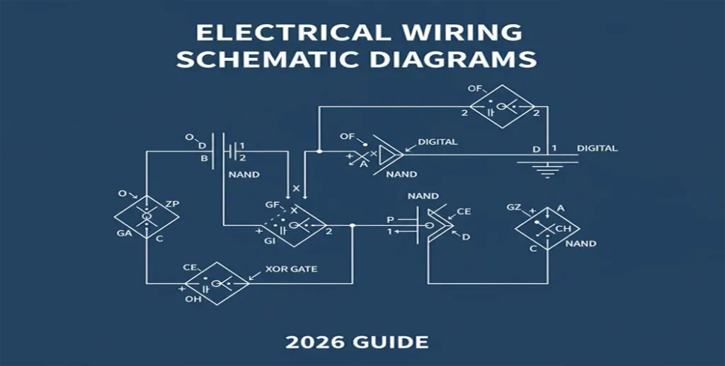
Electrical Wiring Schematic Diagrams
## Table of Contents
– [1. What is an Electrical Wiring Schematic Diagram?](https://procirel.com#what-is-schematic)
– [2. The Universal Language: Common Schematic Symbols](https://procirel.com#symbols-universal-language)
– [3. How to Read a Schematic: Step-by-Step Process](https://procirel.com#how-to-read-schematic)
– [4. Practical Applications: Home to Digital Systems](https://procirel.com#practical-applications)
– [5. Creating Your Own Schematic Diagrams](https://procirel.com#creating-schematics)
– [6. Advanced: Digital Logic Design & Combinational Circuits](https://procirel.com#advanced-digital-logic)
– [7. Safety Considerations & Common Pitfalls](https://procirel.com#safety-pitfalls)
– [8. FAQ Section](https://procirel.com#faq-section)
– [9. Conclusion](https://procirel.com#conclusion)
– [10. Sources & Further Reading](https://procirel.com#sources)
Have you ever stared at the back of an appliance manual looked at a mysterious page filled with lines, symbols, codes and felt completely lost? Or perhaps you have wanted to understand the intricate digital schematic diagram inside your smartphone or design your own electronic ckt? The key to unlocking these mysteries is mastering the schematic diagram.
This comprehensive guide bridges the gap between basic electrical wiring diagrams and advanced[digital electronics](https://procirel. com/). We’ll cover everything from reading a home circuit breaker circuit to designing combinational circuits using logic gates. Whether you’re a homeowner, engineering student, or electronics hobbyist, this 1800+ word guide provides actionable knowledge.
## What is an Electrical Wiring Schematic Diagram?

Electrical Wiring Schematic Diagrams
A schematic diagram (also called[circuit diagram](https://en. wikipedia. org/wiki/Circuit_diagram)or electronic schematic) is an abstract, symbolic representation of an[electrical circuit](/tutorial/electronic-circuits). It shows how components are connected*electrically*, not physically. Think of it as the blueprint for an electrical circuit.
### Hierarchy of Electrical Diagrams
| Diagram Type | Primary Use | Complexity Level | Key Focus |
| — | — | — | — |
| Block Diagram | System overview | Low | Functional relationships |
| Schematic Diagram | Circuit design & analysis | Medium-High | Electrical connections |
| Wiring Diagram | Installation & repair | Medium | Physical wire routing |
| PCB Layout | Manufacturing | High | Physical component placement |
[Flowchart showing progression from block diagram to schematic diagram to wiring diagram to](/api/media/electrical-wiring-schematic-diagram/Comparison-flowchart.
## The Universal Language: Common Schematic Symbols
### Fundamental Electrical Symbols
#### Power & Protection
– Circuit Breaker: Switch symbol in rectangle (represents electric breaker)
– Fuse: Rectangle with line through center
– DC Source: Long/short parallel lines (±)
– Ground: Three horizontal lines ( length)
#### Passive Components
– Resistor: Zig-zag (US) or rectangle (IEC)
– Capacitor: Parallel lines or curved plate
– Inductor: Loops or solid rectangle
– Transformer: Two inductors with coupling
### Digital Logic Gate Symbols (Critical for Digital Electronics)
| Gate Type | Symbol Shape | Boolean Expression | Truth Table Key | Application in Combinational Circuit |
| — | — | — | — | — |
| AND Gate | D-shaped | Y = A·B | Output 1 only if ALL inputs 1 | Enable/control circuits |
| OR Gate | Curved back | Y = A+B | Output 1 if ANY input 1 | Signal multiplexing |
| NAND Gate | AND + circle output | Y = A·B’ | Output 0 only if ALL inputs 1 | Universal gate for any digital schematic diagram |
| XOR Gate | OR + extra curve | Y = A⊕B | Output 1 if inputs DIFFERENT | Binary addition, parity checking |
| NOT Gate (Inverter) | Triangle + circle | Y = A’ | Output inverses input | Signal inversion |
[Animated demonstration of AND, OR, NAND, XOR gates showing output changes with different i](/api/media/electrical-wiring-schematic-diagram/Animated-GIF-showing-how-logic-gate-symbols.
## How to Read a Schematic: Step-by-Step Process
1.
2.
3.
4.
5.
#### Visual Learning: How to Read Schematics
For a step-by-step visual walkthrough of tracing electrical symbols and identifying circuit paths, we recommend this detailed tutorial:
#### Watch: Industrial Wiring Diagrams Explained
If you’re transitioning from basic schematics to complex Industrial Control Panels, this video walkthrough is essential. It covers reading diagrams from top-to-bottom/left-to-right, wire tagging, and standard legends.
#### Supplemental Tutorial: Industrial Diagram Walkthrough
To help you visualize the concepts discussed in this guide. We’ve included this highly-regarded tutorial on industrial wiring standards and diagram reading.
Credits & Source: Video content property of RealPars via YouTube.
[View original video here](https://www.youtube.com/watch?v=GHhcyH99inE).
Pro Tip for Digital Circuits: When analyzing digital schematic diagrams, create a truth table for each logic gate cluster. This reveals the exact Boolean function implemented by that section of the combinational circuit.
## Practical Applications: From Home Wiring to Digital Systems
### Home Electrical System: Circuit Breaker Circuit
A residential circuit breaker circuit schematic shows:
– Main panel with multiple circuit circuit breaker branches
– Overcurrent protection logic
– Ground Fault Circuit Interrupter (GFCI) logic
– Load distribution across phases
### Advanced Digital System: Microcontroller Interface Circuit Design
Modern electronic schematic for Arduino/Raspberry Pi shows:
– Power regulation circuitry
– Clock crystal oscillator circuit
– Programming interface (ICSP/JTAG)
– I/O protection with diodes/resistors
– Communication buses (I2C, SPI, UART)
[Comparison between basic home lighting circuit schematic and advanced microcontroller inte](/api/media/electrical-wiring-schematic-diagram/comparison-of-simple-home-circuit-vs. -complex-digital-circuit-schematic.
## Creating Your Own Schematic Diagrams
### Modern Circuit Design Software Tools
| Software | Best For | Learning Curve | Key Feature for Digital Schematic Diagram |
| — | — | — | — |
| KiCad | Open-source professionals | Medium | Advanced hierarchical schematics |
| Eagle | Hobbyists & startups | Low-Medium | Extensive component libraries |
| Altium Designer | Enterprise & complex designs | High | Unified circuit design environment |
| Fritzing | Beginners & education | Low | Visual breadboard-to-schematic |
### Schematic Creation Workflow
1.
2.
3.
4.
5.
6.
7.
## Advanced Technical Section: Digital Logic Design & Combinational Circuits
### Building Complex Functions from Basic Gates
In digital electronics, we build complex systems using fundamental gates.
#### Half-Adder Circuit Using XOR Gates
A basic combinational circuit for binary addition:
– Sum = A ⊕ B (using XOR gate)
– Carry = A · B (using AND gate)
– Forms foundation for ALU design
*Truth Table:*
A=0,B=0 Sum=0,Carry=0
A=0,B=1 Sum=1,Carry=0
A=1,B=0 Sum=1,Carry=0
A=1,B=1 Sum=0,Carry=1
#### Universal NAND Gate Implementation
Any Boolean function can be implemented using only NAND gates:
– NOT from NAND: Connect both inputs
– AND from NAND: NAND + NOT (NAND)
– OR from NAND: Using De Morgan’s theorem
– XOR from NAND: 4 NAND gates minimum
This universality makes NAND gates fundamental in digital circuit manufacturing.
#### Quick Logic Reference (Boolean Algebra)
| Operation | Gate | Notation | Boolean Law |
| — | — | — | — |
| Complement | NOT | A’ or ¬A | A + A’ = 1 |
| Conjunction | AND | A · B | A · 1 = A |
| Disjunction | OR | A + B | A + 1 = 1 |
### Modern Digital Schematic Diagram Practices
– Hierarchical Design: Top-down approach with multiple schematic sheets
– Bus Notation: Group related signals (DATA[7:0], ADDR[15:0])
– Parametric Components: Symbols with editable parameters
– Design Reuse: Creating and using custom symbol libraries
– Mixed-Signal Design: Combining analog and digital circuits
### Verilog/VHDL Representation of Schematics
In professional circuit design, schematics are often represented in Hardware Description Languages:
Example Verilog for XOR gates circuit:
`module xor_example(input A, B, output Y);
assign Y = A ^ B; // XOR operation
endmodule`
## Safety Considerations & Common Pitfalls
### Critical Safety Warning
NEVER work on live circuits based solely on schematic interpretation.
– Turn off power at main panel and verify with voltage tester
– Understand local electrical codes (NEC/ IEC)
– Match circuit breaker ratings to wire gauge
– Use proper personal protective equipment (PPE)
– Consult licensed professionals for complex installations
### Common Schematic Interpretation Errors
– Ignoring Power/Ground Connections: Missing VCC/GND on IC symbols
– Misreading Logic Levels: Active-low vs active-high signals (e. g.
– Overlooking Hidden Pins: Some IC symbols don’t show all pins
– Confusing Similar Symbols: MOSFET vs BJT, different gate symbols
– Missing Component Values: Resistors without Ω values, capacitors without voltage ratings
## FAQ Section: Your Schematic Diagram Questions Answered
What’s the difference between circuit di …
agram and schematic diagram?
Technically, a circuit diagram is any drawing showing electrical connections. A schematic diagram specifically uses abstract symbols to emphasize function over physical layout. In digital electronics, “schematic” often implies a more detailed, component-level representation.
Why are NAND gates considered universal …
in digital circuits?
NAND gates are functionally complete – you can implement ANY Boolean function (AND, OR, NOT, XOR, etc. ) using only NAND gates. This property makes them ideal for integrated circuit manufacturing, allowing simpler, more uniform chip designs.
How do I choose between XOR gates and ot …
her logic gates in my circuit design?
Use XOR gates when you need: 1) Parity checking/error detection, 2) Binary addition (sum bit). 3) Controlled inversion (A⊕0=A, A⊕1=A’), 4) Comparator circuits (output 1 when inputs differ). For AND/OR functions, use those respective gates.
What software is best for creating digit …
al schematic diagrams?
For beginners: Fritzing. For serious hobbyists: KiCad (free) or Eagle. For professionals: Altium Designer or Cadence OrCAD. Consider your project complexity, budget, and need for PCB integration when choosing.
How can I verify my electronic schematic …
is correct before building?
1) Perform Design Rule Check (DRC) in your CAD software.
2) Create a simulation using SPICE or digital logic simulator.
3) Build a prototype on breadboard.
4) Have another engineer review.
5) For digital circuits, create truth tables for all input combinations.
What’s the relationship between combinat …
ional circuit and sequential circuits?
Combinational circuits have outputs depending only on current inputs (logic gates). Sequential circuits have memory – outputs depend on current inputs AND previous states (flip-flops, registers). Most digital schematic diagrams contain both types.
### Glossary of Technical Terms
Netlist
VCC/GND
Combinational Logic
## Conclusion: Mastering the Blueprint of Modern Electronics
You’ve now journeyed from understanding basic electrical wiring diagrams to analyzing complex digital schematic diagrams with NAND gates and XOR gates.
– Interpret home circuit breaker circuits for safe troubleshooting
– Design and analyze combinational circuits for digital systems
– Create professional electronic schematics using modern tools
– Understand the fundamental building blocks of digital electronics
– Bridge the gap between abstract circuit diagrams and physical implementations
Next Steps: Start with simple schematics using free tools like KiCad. Practice by redrawing existing diagram circuit diagrams, then progress to designing your own electronic ckt projects. Remember that mastery comes through application each schematic you read or create builds your expertise.
*Ready to apply your knowledge? Check out our advanced guide on “PCB Layout from Schematic. Complete Manufacturing Guide” to take your designs from concept to physical reality.
## Sources & Further Reading
– [IEEE Standard 91/91a – Graphic Symbols for Logic Functions](https://www. ieee.
– [All About Circuits – Digital Electronics Textbook](https://www.allaboutcircuits.com/textbook/digital/)– Comprehensive resource on digital circuits
– [NFPA 70: National Electrical Code](https://www. nfpa. org/codes-and-standards/all-codes-and-standards/list-of-codes-and-standards/detail?
– [KiCad Documentation](https://www.kicad.org/docs/)– Complete guide to modern circuit design software
– Wakerly, J. F. (2018). *Digital Design: Principles and Practices. *Pearson.
– [Digital Systems Specialization – Coursera](https://www.coursera.org/specializations/digital-systems)– University-level training in digital circuit design
– [Analog Devices – Schematic Design Tutorials](https://www. analog. com/en/education/education-library/schematics.
– [Logic Gates Tutorial](https://www. electronics-tutorials. ws/logic/logic_1.
## Related guides in this track
– New to Electrical Engineering? Start with the [complete electrical engineering guide](/tutorial/electrical-engineering-complete-guide) it indexes every tutorial in this track.
– [Single-Phase vs Three-Phase Power: The Real Differences](/tutorial/single-phase-vs-three-phase)
– [Power Factor Explained: Why Real Power Is Not Apparent Power](/tutorial/power-factor-explained)
– [Transformer Types and Where Each One Belongs](/tutorial/transformer-types-applications)
– Calculate the numbers: [power calculator](/tools/electrical-power) · [transformer turns ratio calculator](/tools/transformer-turns-ratio)
### Practical example
Re-run the steps above with your own numbers at the bench. Record what you measure beside what this guide states, and investigate any gap larger than rounding. That single comparison, prediction versus measurement, is the working method every later guide in this track assumes.