 Procirel
Logic Gates & Truth Tables: Types, Symbols, and Examples
All 7 logic gates explained with full truth tables, Boolean expressions, real-world applications, De Morgan’s theorem, NAND/NOR universal conversions, CMOS physics, propagation delay, fan-out plus an interactive logic gate simulator.
1. [Home](https://procirel.com/)
3. [Electronics](/tutorial/electronics)
## Key Takeaways
– 7 basic logic gates power all digital systems: AND, OR, NOT (basic), NAND, NOR (universal), XOR, XNOR (arithmetic)
– AND = A·B(output 1 only when ALL inputs are 1) |OR = A+B(1 if ANY input is 1) |NOT = Ā(inverts the input)
– NAND and NOR are Universal Gates any logic function can be built from just one type.
– De Morgan’s Theorem: NOT(A·B) = A’+B’ and NOT(A+B) = A’·B’ the key to simplifying circuits and reducing transistor count
– Propagation Delay: tpd= (tpLH+ tpHL)/2 measures gate speed in nanoseconds; critical for CPU clock frequency limits
– CMOS technology dominates modern digital ICs lower power than TTL, works at 1.8V–5V, 74HC/74LVC series are the industry standard
– XOR is the arithmetic gate it detects difference (A≠B output 1) and is the core of binary adders and parity generators
– NAND flash memory in your SSD/USB drive is named after the NAND gate structure used in its storage cells
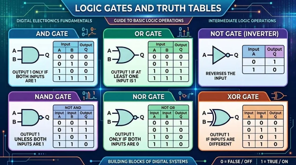
Fig 1. All 7 basic logic gates their IEEE standard circuit symbols, Boolean expressions, and truth table patterns. Together these building blocks compose every digital system from a calculator to a supercomputer.
Quick Engineering Insights
## What Every Student and Engineer Must Know About Logic Gates
NAND is King of Silicon
90%+ of all digital ICs are built using only NAND gates internally. Not because NAND is the simplest but because it requires the fewest transistors per function in CMOS manufacturing. Mastering NAND conversion is the #1 skill for IC designers.
XOR = Half Adder Core
The XOR gate computes binary addition without carry. Combined with AND (for carry), two gates form a complete Half Adder. Four Half Adders chain into a 4-bit Full Adder. Your CPU’s ALU contains millions of these XOR+AND combinations.
Fan-Out Limits Exist
A single gate output cannot drive unlimited inputs. The 74HC series has a fan-out of ~10 (standard CMOS loads). Exceeding fan-out causes voltage degradation and increased propagation delay a critical real-world constraint ignored in textbooks.
CMOS Consumes Power Only When Switching
Unlike TTL, CMOS gates draw near-zero static current. Dynamic power scales with P = C×V²×f proportional to capacitance, voltage squared, and switching frequency. This is why modern CPUs reduce voltage aggressively to save battery.
De Morgan Simplifies Everything
De Morgan’s theorem is the algebraic tool that converts between AND/OR and NAND/NOR implementations. It is the backbone of logic minimization the same mathematics that synthesis tools use to reduce your FPGA or ASIC gate count by 30–50%.
Glitches Are Real Use Timing Diagrams
In sequential circuits, race conditions create nanosecond glitches that cause system failures. Professional engineers use oscilloscopes + timing diagrams to catch these timing violations before the product ships. Simulations miss them; silicon reveals them.
## What Are Logic Gates?
Logic gates are the fundamental building blocks of all digital electronic systems electronic switches that take binary inputs (0 or 1, representing LOW or HIGH voltage) and produce a single binary output based on a defined Boolean logic rule. They translate the mathematical language of[Boolean algebra](https://en. wikipedia. org/wiki/Boolean_algebra)into physical electronic circuits, enabling computers, smartphones, and every digital device to make decisions, perform calculations, and process data.
There are seven basic logic gates
: AND, OR, NOT (the three fundamentals), …
NAND, NOR (the two universal gates), and XOR, XNOR (the arithmetic/special gates). Each has a unique circuit symbol, a Boolean expression, and a truth table that completely defines its behavior for all input combinations.Big Three (Basic)
AND (A·B): all inputs must be 1. OR (A+B): any input can be 1. NOT (Ā): single input, inverts output.
Universal Gates
NAND = NOT-AND: inverse of AND. NOR = NOT-OR: inverse of OR. Both can implement ANY Boolean function alone.
Arithmetic Gates
XOR (A⊕B): output 1 when inputs DIFFER. XNOR (A⊙B): output 1 when inputs are EQUAL. Core of binary adders.
Physical Implementation
Built from MOSFET transistors in CMOS technology. 74HC/74LVC series ICs are the standard. Speed measured by propagation delay (nanoseconds).
## Table of Contents
– [What Are Logic Gates? (Digital Building Blocks)](https://procirel.com#what-are-logic-gates)
– [The Big Three: AND, OR, and NOT Gates](https://procirel.com#basic-gates)
– [Universal Gates: Why NAND and NOR Rule Electronics](https://procirel.com#universal-gates)
– [Advanced Logic: XOR, XNOR, and De Morgan’s Theorem](https://procirel.com#advanced-logic)
– [Digital Logic Performance: Propagation Delay & Power Formulas](https://procirel.com#performance-metrics)
– [How Logic Gates Work Physically: CMOS vs TTL](https://procirel.com#cmos-physics)
– [Industry Standards: 7400 Series, JEDEC & ESD Safety](https://procirel.com#industry-standards)
– [Real-World Applications of Logic Gates](https://procirel.com#real-world-applications)
– [Advanced Diagnostics: Timing Diagrams, Noise Margin & Fan-Out](https://procirel.com#diagnostics-troubleshooting)
– [Advantages and Challenges of Logic Gates](https://procirel.com#advantages-challenges)
– [Experimenting with Logic Gates: Breadboard, Simulators & FPGAs](https://procirel.com#experimenting)
– [Future of Logic: From CMOS to Quantum Logic Gates](https://procirel.com#modern-trends)
– [Interactive Logic Gate Simulator](https://procirel.com#simulator)
– [Logic Gates FAQ: Common Truth Table Questions](https://procirel.com#faqs)
## What Are Logic Gates? (Digital Building Blocks)
Logic gates are the fundamental alphabet of every computer system translating binary signals (1 and 0) into complex decisions via Boolean algebra, named after mathematician George Boole. While traditional computing relies on billions of CMOS transistors switching at incredible speeds, these gates are the conceptual layer that makes all of it intelligible: each gate has a clear, defined, testable behavior that can be expressed mathematically, drawn symbolically, and built physically.
Ever wondered how a computer actually “thinks”? It does not use words it uses a puzzle of logic gates. Inside your smartphone, there are over 16 billion transistors, each acting as a tiny switch (ON = 1, OFF = 0). Logic gates organize these transistors into meaningful operations: add two numbers, check if a condition is true, store a memory bit, or compare two values. Every text message, every game render, every GPS calculation reduces, ultimately, to billions of these gates switching billions of times per second.
[Logic gates symbols and truth tables for AND OR NOT NAND NOR XOR XNOR digital logic](/api/media/basic-logic-gates/Logic_Gates_and_Truth-tables.
Fig 2. Logic gate classification from the three basic gates (AND, OR, NOT) through universal gates (NAND, NOR) to arithmetic gates (XOR, XNOR). Understanding this hierarchy is key to circuit design and minimization.
| Gate Type | Simple Rule | Boolean Expression | Best Use Case |
| — | — | — | — |
| AND Gate | ALL inputs must be 1 for output = 1 | F = A · B | Safety interlocks (keycard AND PIN) |
| OR Gate | ANY input = 1 gives output = 1 | F = A + B | Alarm systems (door OR motion) |
| NOT Gate | Single input output is INVERTED | F = Ā | Signal inversion, enable control |
| NAND Gate | AND followed by NOT universal | F = (A·B)’ | NAND Flash memory cells, CPU logic |
| NOR Gate | OR followed by NOT universal | F = (A+B)’ | SR latches, standby circuits |
| XOR Gate | Output = 1 when inputs DIFFER | F = A ⊕ B | Binary adders, parity generators |
| XNOR Gate | Output = 1 when inputs are EQUAL | F = A ⊙ B | Equality comparators, error detection |
Understanding Binary Logic and Boolean Algebra
Boolean algebra uses only two values: 1 (true / HIGH voltage) and 0 (false / LOW voltage). AND acts like multiplication (1×1=1, 1×0=0), OR like addition with ceiling (0+1=1, 1+1=1), and NOT like negation (NOT 1 = 0). These simple rules applied across billions of transistors produce every computation in modern electronics. The voltage signals in circuits are measured relative to ground: no voltage = 0, full supply voltage = 1. Logic gates are the structured language that maps these voltage states to computation.
## The Big Three: AND, OR, and NOT Gates
These three gates form the complete logical foundation. Mathematically, AND, OR, and NOT are sufficient to implement any Boolean function they are “functionally complete” as a set. Every other gate is built from some combination of these three.
### AND Gate
F = A · B (also written AB)
The AND gate is the strict gatekeeper it outputs 1 only when every single input is 1
. If even one input is 0, the output …
is 0. Think of it as a series circuit with two switches: the light only turns on if both switches are flipped. Symbolically it looks like a D-shape flat on the left (inputs), curved on the right (output).Real-world analogy: A security system requiring*both*a keycard AND a PIN. Neither alone unlocks the door both must be active simultaneously.
#### Truth Table AND Gate
| A | B | F = A·B |
| — | — | — |
| 0 | 0 | 0 |
| 0 | 1 | 0 |
| 1 | 0 | 0 |
| 1 | 1 | 1 |
#### Key Properties
IC Example: 74HC08 (Quad 2-input AND, CMOS) Transistors (CMOS): 4 MOSFETs per 2-input gate Applications:
Security interlocks
Enable gates
Half adder (carry)
Watchdog circuits
### OR Gate
F = A + B
The OR gate is the forgiving gatekeeper it outputs 1 if at least one input is 1
. The only way to get output 0 is if …
ALL inputs are 0. Like a parallel circuit: either switch can turn on the light. The symbol looks like a pointed shield with a curved back.Real-world analogy: A car warning light that activates if the door is open OR the seatbelt is unbuckled any one condition triggers the alert.
#### Truth Table OR Gate
| A | B | F = A+B |
| — | — | — |
| 0 | 0 | 0 |
| 0 | 1 | 1 |
| 1 | 0 | 1 |
| 1 | 1 | 1 |
#### Key Properties
IC Example: 74HC32 (Quad 2-input OR, CMOS) Transistors (CMOS): 4 MOSFETs per 2-input gate Applications:
Alarm systems
Interrupt logic
Multiplexer control
Error flagging
### NOT Gate (Inverter)
F = Ā (also written A’)
The NOT gate also called an inverter takes one input and flips it completely. Input 0 Output 1. Input 1 Output 0. No other gate takes a single input. Symbolically it is a triangle with a small circle (bubble) at the output the bubble is the universal symbol for inversion. The bubble appears on NAND and NOR outputs for the same reason.
#### Truth Table NOT Gate
| A | F = Ā |
| — | — |
| 0 | 1 |
| 1 | 0 |
#### Key Properties
IC Example: 74HC04 (Hex Inverter, CMOS) Transistors (CMOS): 2 MOSFETs (1 PMOS + 1 NMOS) Applications:
Signal inversion
Clock buffers
Active-low enable
Building NAND/NOR
## Universal Gates: Why NAND and NOR Rule Electronics
Fig 3.
### NAND Gate (NOT-AND)
F = (A · B)’ AND output inverted
The NAND gate combines an AND gate followed by a NOT producing the inverse of AND. It outputs 0*only*when all inputs are 1; any other combination gives 1. NAND is the most important gate in digital electronics because it requires the fewest transistors to implement AND-type logic in CMOS only 4 transistors vs. 6 for a separate AND+NOT combination.
#### Truth Table NAND Gate
| A | B | F = (A·B)’ |
| — | — | — |
| 0 | 0 | 1 |
| 0 | 1 | 1 |
| 1 | 0 | 1 |
| 1 | 1 | 0 |
#### Key Properties
IC Example: 74HC00 (Quad 2-input NAND, CMOS) Named product: NAND Flash memory (SSDs, USB drives) Applications:
Universal logic
SR Latch
NAND Flash
CPU logic arrays
### NAND Universal Conversions Build Any Gate from NAND Alone
Engineer’s Secret NAND Universal Gate Conversions
### Why Manufacturers Use Only One Gate Type
Ever wondered why chip manufacturers don’t use all 7 gate types on a single chip? Economies of scale. By designing a chip with only NAND (or only NOR) gates, companies can use a single transistor geometry reducing layout complexity, minimizing process variation, and enabling denser packing.
– NOT from NAND: Connect both inputs together (A·A)’ = A’
– AND from NAND: NAND output NOT (NAND again with both inputs tied) A·B
– OR from NAND: Invert each input (NAND self), then NAND the inverted inputs (A’·B’)’ = A+B (De Morgan)
– NOR from NAND: Build OR from NAND (above), then invert with NAND NOT (A+B)’
– XOR from NAND: Requires 4 NAND gates see timing diagram in Section 9
### NOR Gate (NOT-OR)
F = (A + B)’ OR output inverted

NOR outputs 1*only*when ALL inputs are 0 any 1 input forces the output to 0. This makes NOR ideal for “all-off” detection standby mode detection, zero-input validation, and SR latch construction. NOR is the second universal gate and the basis of CMOS NOR-based logic used in some RISC processor architectures.
#### Truth Table NOR Gate
| A | B | F = (A+B)’ |
| — | — | — |
| 0 | 0 | 1 |
| 0 | 1 | 0 |
| 1 | 0 | 0 |
| 1 | 1 | 0 |
#### Key Properties
IC Example: 74HC02 (Quad 2-input NOR, CMOS) Transistors (CMOS): 4 MOSFETs per 2-input gate Applications:
SR Latch / Flip-flop
Standby detection
Universal logic
Zero-input check
From the Bench Oliver Adam, M.Sc., Lead Editor
I once built a complete alarm system using only NAND gates because I had run out of other ICs mid-project. Working through the Boolean logic to convert every OR, NOT, and AND into NAND equivalents taught me something no textbook had: NAND gates are not just a “universal backup. ” They are the natural language of silicon. After that project, my NAND gate conversions became second nature and my designs got noticeably smaller and cheaper.
Oliver Adam, M.Sc., Lead Editor · 8+ years electronics education.
## Advanced Logic: XOR, XNOR, and De Morgan’s Theorem
### XOR Gate (Exclusive OR)
F = A ⊕ B = A’B + AB’

XOR outputs 1 when the inputs are different
(one is 0, the other is 1). When both …
inputs are the same both 0 or both 1 output is 0. This “difference detection” property makes XOR the arithmetic gate: it performs binary addition without the carry. Symbolically it looks like an OR gate with an extra curved line on the input side.Analogy: A hallway light controlled by two switches flipping either one changes the state, but flipping both leaves the state unchanged.
#### Truth Table XOR Gate
| A | B | F = A⊕B |
| — | — | — |
| 0 | 0 | 0 |
| 0 | 1 | 1 |
| 1 | 0 | 1 |
| 1 | 1 | 0 |
#### Key Properties
IC Example: 74HC86 (Quad 2-input XOR, CMOS) Half Adder: Sum = A⊕B, Carry = A·B Applications:
Binary adder (Sum bit)
Parity generator
Error detection (CRC)
Cipher/encryption
### XNOR Gate (Exclusive NOR)
F = A ⊙ B = A’B’ + AB

XNOR is XOR followed by NOT it outputs 1 when inputs are equal(both 0 or both 1), and 0 when they differ. XNOR is the equality detector: if A = B, output is 1. This makes it the natural choice for digital comparators checking whether two binary values match bit-for-bit.
#### Truth Table XNOR Gate
| A | B | F = A⊙B |
| — | — | — |
| 0 | 0 | 1 |
| 0 | 1 | 0 |
| 1 | 0 | 0 |
| 1 | 1 | 1 |
#### Key Properties
IC Example: 74HC7266 (Quad 2-input XNOR) Complementary: XNOR = NOT XOR (A⊕B)’Applications:
Digital comparator
Equality checker
Password matching
Phase detector (PLLs)
### De Morgan’s Theorem The Circuit Simplification Superpower
De Morgan’s Theorem is the single most powerful tool in Boolean algebra for circuit simplification and gate conversion. It states:
De Morgan’s Theorem Two Laws
NOT(A · B) = A’ + B’ | NOT(A + B) = A’ · B’
Law 1: The complement of a product = sum of complements (NAND OR of inverted inputs)
Law 2: The complement of a sum = product of complements (NOR AND of inverted inputs)
Practical use:
Convert NAND/NOR expressions into AND/O …
R form (or vice versa) for minimization Example: (A·B·C)’ = A’ + B’ + C’ useful for simplifying 3-input NAND gates
#### De Morgan’s Theorem Why It Matters for CPUs and AI Chips
De Morgan’s theorem is the algebraic core of logic synthesis tools (Synopsys Design Compiler, Vivado). When you write RTL code in Verilog/VHDL, the synthesis tool applies De Morgan transformations thousands of times to minimize the gate count of your design. In modern CPUs, this reduces die area by 15–30%. In 2026, Huawei’s CMOS-based ternary circuits extend De Morgan’s theorem to ternary logic (0, ½, 1), achieving 30% gate count reduction and 20% power savings for AI neural network edge computing.
## Digital Logic Performance: Propagation Delay & Power Formulas
A gate is not defined solely by its truth table its speedandpower consumption are equally critical in real circuit design. Engineers use these quantitative metrics to select the correct IC family (74HC vs. 74LVC) for their application.
Propagation Delay Gate Speed Measurement
tpd= (tpLH+ tpHL) / 2
tpd= Average propagation delay (nanoseconds, ns)
tpLH= Low-to-High transition delay (input changes output goes HIGH)
tpHL= High-to-Low transition delay (input changes output goes LOW)
74HC series at 5V: tpd≈ 7–9 ns |74LVC at 3.3V: tpd≈ 4–6 ns
Minimizing tpdis critical for maximizing microprocessor clock speed
Power-Delay Product Efficiency Gold Standard
PDP = Pavg× tpd
PDP = Power-Delay Product (Joules per switching event lower = better)
Pavg= Average dynamic power per gate = C × V² × f
C = Gate capacitance | V = Supply voltage | f = Switching frequency
Key insight:
Reducing voltage from 5V to 3.3V reduce …
s dynamic power by 56% (V² relationship) Modern CMOS: PDP ≈ 1–10 femtojoules per gate why billions of gates fit in a portable device
| IC Family | Technology | Supply Voltage | tpd(typical) | Best For |
| — | — | — | — | — |
| 74HC | High-Speed CMOS | 2V – 6V | 7–9 ns @ 5V | General digital, 5V systems |
| 74LVC | Low-Voltage CMOS | 1.65V – 3.6V | 4–6 ns @ 3.3V | Modern microprocessor I/O, 3.3V systems |
| 74ALVC | Advanced LVC | 1.65V – 3.6V | 2–3 ns @ 3.3V | High-speed bus interfaces, DDR memory |
| 74F (Fast TTL) | Bipolar TTL | 4.5V – 5.5V | 3–5 ns | Legacy high-speed TTL applications |
## How Logic Gates Work Physically: CMOS vs TTL
Logic gates are built from transistors inside integrated circuits. Understanding the underlying technology CMOS(Complementary Metal-Oxide-Semiconductor) vs.TTL(Transistor-Transistor Logic) explains why modern devices are so fast, small, and power-efficient.
CMOS NOT Gate (Inverter) 2-Transistor Implementation
VDD(+5V)PMOS(Pull-up)Input ANMOS(Pull-down)GND (0V)Output F = ĀInput A = 1 (HIGH):PMOS: OFF (blocks VDD)NMOS: ON (connects GND)Output = 0 (LOW)Input A = 0 (LOW):PMOS: ON (connects VDD)NMOS: OFF (blocks GND)
In CMOS, each gate uses complementary pairs of PMOS and NMOS transistors. When input is HIGH: the NMOS turns ON (pulls output to GND = 0) and the PMOS turns OFF. When input is LOW: PMOS turns ON (pulls output to VDD = 1) and NMOS turns OFF. At any static state, one transistor is always OFF creating a near-infinite resistance path between VDD and GND. This is why CMOS draws essentially zero static current the only power consumed is during transitions (switching current to charge/discharge gate capacitances).
### CMOS Advantages
– Near-zero static power consumption
– Works at 1.8V, 3.3V, or 5V supply
– Very high input impedance (virtually no input current)
– Full rail-to-rail output swing (0 to VDD)
– Scales well modern 3nm CMOS gates work
– Lower heat generation than TTL
### CMOS Limitations
– Susceptible to ESD damage (requires grounding straps)
– Latch-up risk from voltage transients above VDD
– Dynamic power scales with f×V² high-freq designs get hot
– Slower than bipolar TTL at same voltage (historically)
– Gate oxide breakdown from overvoltage
## Industry Standards: 7400 Series, JEDEC & ESD Safety
All basic logic gates are manufactured under rigorous standards to ensure compatibility, reliability, and interoperability across designs and manufacturers.
### Key IC Series and JEDEC Standards
– 74HC (High-Speed CMOS): The industry workhorse for 5V digital designs. Offers low static power but higher dynamic power. Pin-compatible with the original 7400 TTL series enabling easy modernization of legacy designs.
– 74LVC (Low-Voltage CMOS): Used in modern 3. 3V and 1. 8V systems. Optimized for low-voltage, high-speed switching to minimize power-delay product (PDP). Common in Arduino shield designs and microprocessor interface logic.
– JEDEC Standards: Logic gates must comply with JEDEC (Joint Electron Device Engineering Council) standards which dictate pin configurations, operating temperature ranges, maximum rated voltages, and logic level thresholds (VIH, VIL, VOH, VOL). JEDEC compliance ensures a 74HC00 from Texas Instruments is interchangeable with one from Nexperia or Toshiba.
### Electrostatic Discharge (ESD) and Latch-Up Safety
ESD and Latch-Up Real Failure Modes
ESD (Electrostatic Discharge):
CMOS gates are highly susceptible to ES …
D damage a static spark from handling can permanently destroy the thin gate oxide of MOSFET transistors. Always use anti-static wrist straps when handling ICs, store in anti-static bags, and use ESD-safe workbenches. Most CMOS ICs have built-in ESD protection diodes, but these only handle moderate ESD not direct contact with charged human body or tools.Latch-Up: An internal failure where parasitic transistors inside the CMOS substrate create a low-resistance path from VDD to GND effectively short-circuiting the power supply. Usually triggered by voltage spikes above VDD or below GND on any I/O pin (e. g. , hot-plugging a signal). Prevention: add series resistors (100–500Ω) on inputs, use TVS diodes on external-facing pins, and ensure power-up sequencing is correct.
| Standard | Organization | Scope |
| — | — | — |
| JEDEC JESD8C | JEDEC | Interface standards for logic IC voltage levels VIH, VIL, VOH, VOLspecifications |
| IEC 61000-4-2 | IEC | ESD immunity testing for electronic equipment defines test levels and procedures |
| MIL-STD-1686 | US DoD | ESD control requirements for military/aerospace electronic equipment handling |
| IPC-A-610 | IPC | PCB assembly quality includes ESD control requirements for solder assembly of CMOS ICs |
## Real-World Applications of Logic Gates
[Applications of logic gates in real world devices and circuits CPUs, smartphones, alarm sy](/api/media/basic-logic-gates/Applications-of-Logic-Gates-in-the-Real-World-1024×559.
Fig 4.
| Application | Gates Used | Function |
| — | — | — |
| CPU Arithmetic Logic Unit (ALU) | XOR, AND, OR, NOT | Addition (Half/Full Adder), subtraction, comparison |
| NAND Flash Memory (SSD/USB) | NAND | Floating-gate NAND cell structure stores charge for data bits |
| SR Latch (Memory Bit) | NAND or NOR | Stores one bit; used in registers, flip-flops, SRAM cells |
| Security Systems | AND, XOR | AND: all conditions must be met. XOR: compare input to stored code |
| Automotive ABS/AirbagECU | AND, OR, NOT | Multi-sensor fusion trigger only when multiple conditions align |
| Parity Generator (CRC/UART) | XOR chain | Detect single-bit transmission errors XOR of all data bits |
| Multiplexer / Demux | AND, OR, NOT | Route signals based on select inputs core of bus switching |
| IoT Sensor Interface | AND, NOT | Enable sensors only when power and wake conditions are both met |
Case Study The XOR Half Adder: Binary Addition in 2 Gates
### How Your Calculator Does 1 + 1 in Silicon
Binary addition of two single bits requires exactly two logic gates: XOR and AND. The XOR gate produces the Sum bit
(1+1 = 0, carry 1; 0+1 = 1, no carry; 1+ …
0 = 1, no carry; 0+0 = 0, no carry). The AND gate produces the Carry bit
(carry is 1 only when both inputs are 1) …
. Together they form a Half Adder the simplest binary addition circuit.
Four Half Adders chained together form a 4-bit Full Adder. Eight Full Adders form a byte-wide adder. Your CPU’s ALU contains hundreds of these chained adder circuits, executing addition operations in a single clock cycle at GHz frequencies. The entire arithmetic capability of modern computing reduces, ultimately, to XOR and AND gates.
Sum = A ⊕ B | Carry = A · B Half Adder complete
## Advanced Diagnostics: Timing Diagrams, Noise Margin & Fan-Out
Fig 5. Logic gate diagnostics oscilloscope timing diagram showing propagation delay between input transition and output response. Glitches, clock skew, and noise margin violations are visible at this level of analysis.
### Using Timing Diagrams for Fault Isolation
Timing diagrams are the essential diagnostic tool for sequential logic circuits showing all signal states versus time simultaneously.
– Glitches: Unintended short pulses (often <10 ns) caused by race conditions two signal paths with different propagation delays arriving at a gate at different times. Visible on oscilloscope as narrow spikes between expected output states. Prevention: add small delay elements or redesign the combinational path.
- Clock Skew: The clock signal arrives at different flip-flops at slightly different times due to unequal routing distances. Diagnosed by measuring clock rising edge arrival times across multiple chip pins. Problematic when skew exceeds the setup/hold time margin of flip-flops.
– Metastability: A flip-flop’s output becomes indeterminate when input changes too close to the clock edge. The output hovers between 0 and 1 for an unpredictable time causing downstream logic failures. Mitigated by synchronizers (double flip-flop chains) when crossing clock domains.
### Noise Margin and Fan-Out Constraints
Noise Margin Gate Robustness
NMH= VOH(min)− VIH(min)NML= VIL(max)− VOL(max)
NMH= High-level noise margin | NML= Low-level noise margin
VOH= Minimum output HIGH voltage | VIH= Minimum input HIGH threshold
VOL= Maximum output LOW voltage | VIL= Maximum input LOW threshold
74HC at 5V: NMH≈ NML≈ 1.0–1.5V good noise immunity
Noise margin represents how much voltage noise a gate can tolerate without producing a wrong output
Fan-Out: The Real-World Constraint Textbooks Skip
Fan-out is the maximum number of gate inputs that a single gate output can reliably drive. For 74HC series: fan-out ≈ 10 (10 standard CMOS inputs). Exceeding fan-out causes: reduced output voltage swing (NM decreases), increased propagation delay (higher capacitive load to charge), and potential logic errors. In real designs with long PCB traces, the trace capacitance further reduces effective fan-out. Solution: use buffer ICs (74HC244/245) to drive high-fanout nets.
## Advantages and Challenges of Logic Gates
[Advantages and limitations of logic gates in digital electronics](/api/media/basic-logic-gates/Advantages-and-Limitations-of-Logic-Gates-1024×559.
Fig 6. Logic gates in complex digital systems advantages in reliability and scalability vs.
### Advantages
– Noise immunity: Digital signals resist analog interference clear 0/1 states recover from noise that would corrupt analog signals
– Predictable behavior: Truth tables completely define output for every input no ambiguity, no variation between chips
– Infinite scalability: Combine any number of gates to build any function from a calculator to a supercomputer, same principles
– Low static power (CMOS): Near-zero current when not switching why your phone battery lasts days, not hours
– Standardization: 74-series ICs are globally interchangeable a 74HC00 from any manufacturer works identically
– Miniaturization: Modern 3nm process packs 100M+ transistors per mm² more logic in less space every generation
### Challenges
– Propagation delay: Every gate adds nanoseconds in deep logic chains, cumulative delay limits maximum clock frequency
– Dynamic power: Power = C×V²×f at GHz frequencies and billions of gates, heat dissipation becomes a primary engineering challenge
– Not native for analog: Cannot directly process analog signals without ADC conversion mixed-signal systems need both domains
– Radiation sensitivity: In space and nuclear environments, high-energy particles can flip bits (Single Event Upsets) requires radiation-hardened (rad-hard) ICs
– ESD vulnerability: Static discharge can permanently damage CMOS gate oxide requires careful handling protocols
## Experimenting with Logic Gates: Breadboard, Simulators & FPGAs
[Experimenting with basic logic gates breadboard and truth tables 7400 IC wiring](/api/media/basic-logic-gates/Experimenting-with-Basic-Logic-Gates-1024×559.
Fig 7.
The best way to master logic gates is hands-on experimentation.
| Method | Tools Needed | Best For | Cost |
| — | — | — | — |
| Breadboard + 7400 ICs | Breadboard, 74HC00/08/32, LEDs, resistors, 5V supply | Physical truth table verification, real timing measurement | $5–$15 |
| Logic Simulator (Logisim) | Free Logisim-Evolution software | Complex circuit design and simulation without hardware | Free |
| Online Simulator (CircuitVerse) | Browser circuitverse.org | Quick truth table testing, sharing circuit designs | Free |
| Arduino / Microcontroller | Arduino Uno or ESP32 | Software implementation of logic gates for rapid prototyping | $5–$20 |
| FPGA (Xilinx/Intel) | Basys 3 or DE10-Lite FPGA board | Program logic directly in hardware real silicon implementation | $50–$150 |
Hands-On Project AND Gate Breadboard Demo
### Build a Physical AND Gate in 5 Minutes
Components:
74HC08 IC (Quad 2-input AND), 2× switch …
es (or jumper wires), 1× LED, 1× 330Ω resistor, 5V power supply, breadboard.Wiring:
Connect IC pin 14 to +5V, pin 7 to GND. …
Connect two switches to pins 1 and 2 (inputs A and B). Connect pin 3 (output) through 330Ω resistor to LED anode, LED cathode to GND.Test: Toggle both switches through all four input combinations (00, 01, 10, 11). Observe that the LED lights*only*when BOTH switches are ON perfectly matching the AND truth table. This physical verification builds intuition that no simulator can fully replace.
## Future of Logic: From CMOS to Quantum Logic Gates
Logic gate technology is advancing rapidly beyond classical CMOS driven by the demands of AI hardware, quantum computing, and ultra-low-power edge devices.
### Cryogenic CMOS for Quantum Computing
Classical CMOS control electronics must operate near the quantum processor at cryogenic temperatures (4 Kelvin, close to absolute zero). Cryo-CMOS(pioneered by SemiQon/VTT and Intel) integrates standard logic gate structures that function reliably at 4K. This reduces the massive wiring harness connecting room-temperature electronics to quantum chips enabling quantum processors to scale from dozens to thousands of qubits. SemiQon’s cryo-CMOS chip (2025 EARTO Innovation Award winner) supports 5,000-gate circuits on IBM Nighthawk architecture.
### Ternary Logic: Beyond Binary
Standard CMOS uses binary (0 and 1). Ternary logic uses three values (0, ½, 1) Huawei’s 2026 patented CMOS-based ternary circuits reduce gate count by 30% and power by 20% for AI neural network edge computing. De Morgan’s theorem extends to ternary logic with modified rules. While not yet commercially mainstream, ternary logic represents a potential leap beyond the power-per-computation limits approaching in standard binary CMOS.
### Error-Transparent Quantum Gates
In quantum digital design, logic gates evolve into error-transparent gates using parity-nested operations on binomial-encoded qubits enabling fault-tolerant quantum algorithms across networked processors. Quantinuum Helios has demonstrated 99. 9975% fidelity two-qubit gates a game-changer for distributed quantum computing that will eventually require rethinking the entire logic gate paradigm from its CMOS foundations.
2026 Expert Insight: De Morgan in AI Chips
De Morgan’s theorem originally a 19th-century Boolean algebra result now optimizes ternary logic in cryo-CMOS AI chips, reducing quantum cost and latency in error-corrected qubit operations. The mathematical principle that simplifies your student circuit exercise is the same one pushing the frontier of quantum computing today.
## Interactive Logic Gate Simulator
Select a gate type, toggle inputs A and B, and see the output update in real time with the Boolean expression. Perfect for verifying truth tables.
Gate Type:
AND Gate F = A · BOR Gate F = A + BNOT Gate F = Ā (input A only)NAND Gate F = (A · B)’NOR Gate F = (A + B)’XOR Gate F = A ⊕ BXNOR Gate F = A ⊙ B
A =
0
B =
0
Output F
0
F = A · B = 0 · 0 = 0
## Conclusion: Logic Gates The Alphabet of Digital Intelligence
Logic gates transform simple binary signals into the complex systems behind calculators, CPUs, smartphones, and AI processors. Mastering their truth tables, Boolean expressions, De Morgan’s theorem, and physical implementation gives you a clear window into how every digital machine makes decisions at the most fundamental level.
The journey from a single AND gate to a 16-billion-transistor SoC is a journey of composition combining simple rules into structures of infinite complexity. Whether you are building your first breadboard circuit with a 74HC08, programming logic into an FPGA, or designing a cryo-CMOS quantum interface chip, the seven gates covered in this guide remain the indivisible atoms of your digital universe.
Start experimenting wire up a breadboard, open Logisim, or try the interactive simulator above. The best way to master logic gates is to use them. Visit[Procirel. com](https://procirel. com/)for more digital electronics guides and start building today.
## Logic Gates FAQ: Common Truth Table Questions
1. What are logic gates in simple terms?
Logic gates are the fundamental building blocks of digital circuits electronic switches that process binary signals (0 and 1) based on Boolean logic rules to perform computational tasks. Each gate takes one or more binary inputs and produces a single binary output. For example, an AND gate outputs 1 only when both inputs are 1; an OR gate outputs 1 when at least one input is 1. Billions of these gates, organized into complex networks, constitute every digital device from a calculator to a supercomputer.
2. How many types of logic gates are there?
There are seven primary logic gates: AND, OR, NOT (the three basic gates), NAND, NOR (the two universal gates), and XOR, XNOR (the arithmetic/special gates). These seven form the complete set used in digital design. Additional specialized gates exist (like BUFFER, tri-state gates, Schmitt trigger inputs) but they are derived from or variations of these seven fundamentals.
3. Why are NAND and NOR called “Universal Gates”?
They are called universal because any Boolean logic function no matter how complex can be implemented using only NAND gates or only NOR gates. NOT (NAND with inputs tied together), AND (two NANDs), OR (three NANDs), XOR (four NANDs), and any combinational function can all be built from a single gate type. This property makes chip manufacturing more efficient: instead of fabricating 7 different transistor architectures, a manufacturer uses only one, reducing cost and increasing reliability through standardization.
4. What technology is used to build modern logic gates?
Modern gates are primarily built using CMOS (Complementary Metal-Oxide-Semiconductor) technology using complementary pairs of PMOS and NMOS MOSFETs. CMOS draws near-zero static current (only during switching transitions), enabling billions of gates to operate in battery-powered devices. In 2026, leading process nodes are 3nm (TSMC N3, Samsung 3GAE). Specialized applications use: GaN (gallium nitride) for power electronics, SiGe (silicon-germanium) for RF/microwave, and cryo-CMOS for quantum computing control at 4 Kelvin.
5. How does binary math relate to logic gates?
Binary math uses only 0 and 1, corresponding to the OFF and ON electrical states of transistors. Boolean algebra defines operations on these binary values: AND (multiplication: 1×1=1), OR (saturating addition: 1+1=1, not 2), NOT (negation: NOT 1 = 0). Logic gates physically implement these Boolean operations an AND gate is a circuit that computes the Boolean AND of its input voltages. Building adders, comparators, and multipliers from gates is the process of translating binary arithmetic operations into Boolean expressions and then into gate networks.
6. What is the difference between an OR gate and an XOR gate?
Both output 1 for single-1 inputs, but they differ for the 1-1 case: OR gate
outputs 1 for inputs 01, 10, AND 11 any …
input being 1 is sufficient.XOR (Exclusive OR) outputs 1 only when the inputs are DIFFERENT (01, 10) it outputs 0 when both are 1. This “exclusive” behavior makes XOR the sum bit of binary addition (1+1 = 0 with carry 1) and the foundation of parity generators and cryptographic operations where detecting difference between values is key.
7. Where are logic gates used in real life?
Logic gates are everywhere: in your smartphone’s processor (billions of gates computing every operation), calculator’s ALU (XOR and AND gates performing binary arithmetic), digital watches (gates counting oscillator pulses), automated street lights (AND gates combining darkness sensor with timer), washing machines (gates checking water level AND temperature AND door lock before starting), NAND Flash storage in every SSD and USB drive, anti-lock braking systems in cars, pacemakers, satellite navigation receivers, and every other digital device.
8. How does De Morgan’s Theorem help in circuit design?
De Morgan’s Theorem (NOT(A·B) = A’+B’ and NOT(A+B) = A’·B’) allows engineers to simplify complex Boolean expressions and convert between AND/OR implementations and NAND/NOR implementations. This is critical because: (1) NAND and NOR are cheaper to build in silicon. (2) Converting a complex expression to all-NAND minimizes transistor count; (3) Logic synthesis tools apply De Morgan transformations thousands of times to minimize ASIC/FPGA designs. In modern CPU design, systematic De Morgan optimization reduces die area by 15–30% compared to naive AND/OR implementations.
9. Can logic gates be built without transistors?
Yes logic gates can be implemented using: diodes (diode logic used in early 1950s computers), mechanical relays (relay logic still used in industrial control for high-voltage switching), fluidics (fluid logic gates used in harsh chemical environments where electronics fail), optical fibers (optical logic active research area for ultra-fast photonic computing), and even DNA molecules (biological computing research stage). However, silicon MOSFET transistors remain the most efficient, fastest, smallest, and cheapest implementation for microelectronics which is why all consumer digital devices use CMOS.
10. Why is mastering logic gates essential for AI and Robotics?
AI processors (NPUs, TPUs) and robot controllers make real-time decisions requiring ultra-low latency at the hardware level. Understanding logic gates is essential because: (1) AI hardware acceleration is built from specialized gate arrays optimized for matrix multiply operations; (2) FPGA-based AI inference uses programmable logic gate arrays reconfigured for specific neural network architectures. (3) Edge AI chips (running ML models on sensors) require designing gate-level circuits that compute inferences in microseconds at milliwatt power budgets; (4) Autonomous robot safety systems use logic gate interlocks for guaranteed response times that software cannot provide.
Written & Reviewed By
### Oliver Adam, M.Sc.
Lead Editor · Digital Logic & Electronics Specialist
Oliver holds a Master’s degree and has over 8 years of experience teaching digital logic, Boolean algebra, and electronics engineering to students and professionals. He specializes in bridging the gap between abstract theory and practical circuit design from truth tables to real silicon implementation. Every guide is verified against real circuit behavior and industry standards.
8+ Years Education
M.Sc. Stanford University
Digital Logic Expert
FPGA Design
CMOS/VLSI
Reviewed by engineer technically verified March 2026 ·[Editorial policy](https://procirel.com#)
## Continue Learning on Procirel
[Microcontrollers
ESP32 vs Raspberry Pi 5: Which is Best? 2026 Guide
Implement logic gate functions in code on the right microcontroller platform](/tutorial/esp32-vs-raspberry-pi)
[Boolean Algebra
Sum of Products: Complete SOP Guide with Examples
Convert truth tables into AND-OR logic circuits using SOP minimization](/tutorial/sum-of-products)
[Active Devices
MOSFET as a Switch: Formulas & Design
The MOSFET transistors that physically build every CMOS logic gate](/tutorial/mosfet-as-switch)
[Circuit Fundamentals
Electron Devices and Circuits: Complete Guide
Passive/active components, BJT, RC circuits the full electronics foundation](/tutorial/electron-devices-and-circuits)
[Electronics Hub
All Electronics Tutorials Procirel
Browse the complete Procirel library of digital logic and electronics guides](/tutorial/electronics)
[PCB Design
PCB Design Guides Procirel
Design PCBs for your 7400-series logic gate circuits with proper grounding](/tutorial/pcb-design)
[Signal Integrity
Signal Noise in Electrical Circuits
How noise affects logic gate noise margin and digital circuit reliability](/tutorial/signal-noise-electrical-circuites)
[Arduino
Arduino Tutorials Procirel
Implement logic gate functions in Arduino code for rapid prototyping](/tutorial/arduino)
First Post in Series
[ESP32 vs Raspberry Pi 5: Which is Best for Your Project? 2026 Guide](/tutorial/esp32-vs-raspberry-pi)
1 thought on “Logic Gates Guide: Truth T …
ables & Circuit Symbols”
Pingback:[The Ultimate Comparison: ESP32 vs Raspberry Pi](/tutorial/esp32-vs-raspberry-pi)
## Technical References
– 1Boole, G. (1854)*An Investigation of the Laws of Thought*Walton and Maberly Original formulation of Boolean algebra [Foundational Work]
– 2Mano, M.M. & Ciletti, M.D.*Digital Design, 5th Edition*Pearson Logic gate theory, truth tables, Boolean minimization [Academic Textbook]
– 3Wikipedia[Boolean Algebra](https://en.wikipedia.org/wiki/Boolean_algebra)Mathematical foundations of digital logic [Reference]
– 4Wikipedia[Circuit Diagram](https://en.wikipedia.org/wiki/Circuit_diagram)Schematic representation standards for logic gates [Reference]
– 5Texas Instruments[74HC/HCT Logic Gates Datasheet](https://www. ti. com/lit/sg/sdyu001ab/sdyu001ab.
– 6JEDEC JESD8C*Interface Standard for Nominal 3V/3.3V Supply Digital Integrated Circuits*Logic level voltage threshold standards [Industry Standard]
– 7Razavi, B.*Design of Analog CMOS Integrated Circuits*McGraw-Hill CMOS transistor physics, gate construction, power analysis [Academic Textbook]
– 8IEC 61000-4-2*Electromagnetic Compatibility: Electrostatic Discharge Immunity Test*ESD protection standards for electronic equipment [International Standard]
All truth tables, Boolean expressions, and timing specifications verified against Mano & Ciletti (2012), Texas Instruments 74HC datasheet family, and JEDEC JESD8C. Gate application examples represent typical digital engineering practice.
window. lazyLoadOptions=Object. assign({},{threshold:300},window. lazyLoadOptions||{});! function(t,e){“object”==typeof exports&&”undefined”! =typeof module? module. exports=e():”function”==typeof define&&define. amd? define(e):(t=”undefined”! =typeof globalThis? globalThis:t||self). LazyLoad=e()}(this,function(){“use strict”;function e(){return(e=Object. assign||function(t){for(var e=1;e
### Practical example
Take the first measured row from the table above: 0 corresponds to 0 under 0. Reproduce that configuration at the bench, record your own value beside it, and any meaningful gap tells you which tolerance or assumption deserves a closer look. Cross-check the arithmetic with the linked calculator before trusting either number.
## Keep going with this track
– The complete electronics fundamentals guide: [Electronics Fundamentals complete guide](/tutorial/electronics-fundamentals-complete-guide)
– Read next: [diodes and transistors explained: the two semiconductor families](/tutorial/diodes-and-transistors-explained)
– Also in this track: [passive components: resistors, capacitors and inductors compared](/tutorial/passive-components)
– Continue with: [the pn junction diode: physics, curves and applications](/tutorial/pn-junction-diode)
– Calculate as you go: [Ohm’s law calculator](/tools/ohms-law) · [resistor colour code decoder](/tools/resistor-color-code) · [RC time constant tool](/tools/rc-time-constant)
– Bookmark this page against the day a measurement surprises you. Most readers return to the table and the mistake list first, and that is the correct order.
## Frequently asked questions
Universal Gates: Why NAND and NOR Rule Electronics?
NAND Gate (NOT-AND)
F = (A · B)’ AND output inverted
The NAND gate combines an AND gate followed by a NOT producing the inverse of AND . It outputs 0 only when all inputs are 1; any other combination gives 1.
Advanced Logic: XOR, XNOR, and De Morgan’s Theorem?
XOR Gate (Exclusive OR)
F = A ⊕ B = A’B + AB’

XOR outputs 1 when the inputs are different (one is 0, the other is 1). When both inputs are the same both 0 or both 1 output is 0.
The Big Three: AND, OR, and NOT Gates?
Mathematically, AND, OR, and NOT are sufficient to implement any Boolean function they are “functionally complete” as a set. AND Gate
F = A · B (also written AB)
The AND gate is the strict gatekeeper it outputs 1 only when every single input is 1 .